Nitride semiconductor light emitting device

a light-emitting device and nitride technology, applied in solid-state devices, instruments, data processing applications, etc., can solve the problems of low light-emitting efficiency per light-emitting area, low current density, low area efficiency, etc., to improve the current-spreading effect, reduce contact resistance, and boost light-emitting efficiency

Inactive Publication Date: 2006-08-31
SAMSUNG ELECTRO MECHANICS CO LTD
View PDF9 Cites 118 Cited by
  • Summary
  • Abstract
  • Description
  • Claims
  • Application Information

AI Technical Summary

Benefits of technology

[0015] The present invention has been made to solve the foregoing problems of the prior art and it is therefore an object of the present invention to provide a flip-chip nitride semiconductor Light Emitting Device (LED) having a new electrode structure capable of arranging bonding pads to ensure easy flip chip bonding process and stable support of the LED, and also enhancing current spreading efficiency.
[0019] To improve current spreading effect, each of the first and second electrode fingers may comprise a portion extended along a top edge of the light emitting structure toward adjacent one of the bonding pads having different polarity.
[0020] Preferably, to boost light emitting efficiency in a flip-chip bonding, the nitride semiconductor LED may further comprise a reflexive ohmic contact layer on the second conductivity-type nitride semiconductor layer to reduce contact resistance, wherein the second electrodes are formed on the reflexive ohmic contact layer.

Problems solved by technology

Also, the planar nitride LED has low light emitting efficiency per light emitting area.
The nitride semiconductor LED exhibits low current density per unit area owing to its planar structure, and also has low area efficiency resulting from the small light emitting area.
Such disadvantages are more manifested in a large-sized LED (e.g. 1000 μm×1000 μm) for lighting device.
This complicates a bonding process and renders it difficult to support the LED stably.
For example, a flip-chip process of the p-bonding pad close to a center is difficult, and asymmetrical arrangement of electrodes on the total area requires too great a number of bonding pads to support the LED stably.

Method used


Image

  • Nitride semiconductor light emitting device
  • Nitride semiconductor light emitting device
  • Nitride semiconductor light emitting device

Examples


Embodiment Construction

[0030] Preferred embodiments of the present invention will now be described in detail with reference to the accompanying drawings.

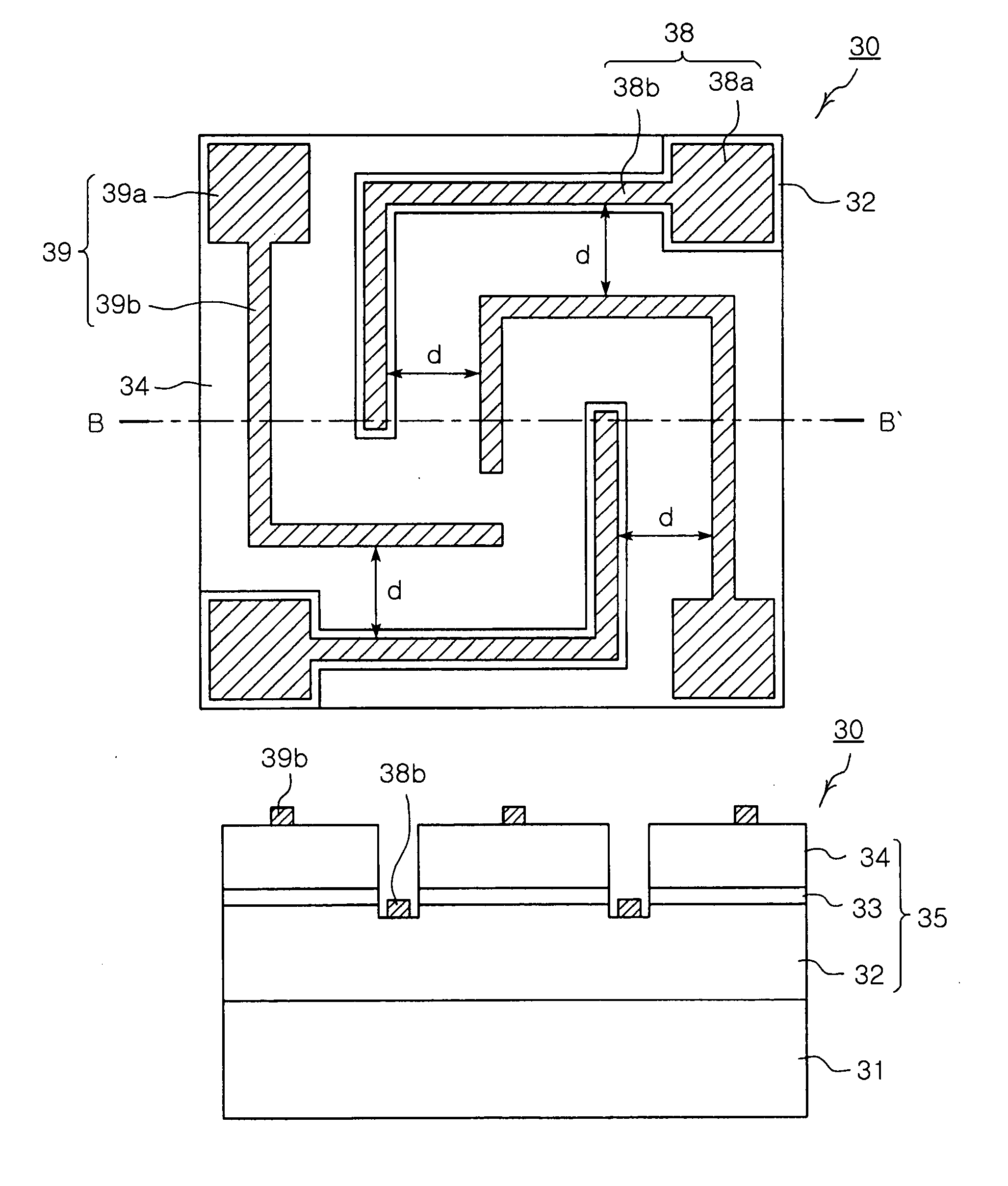
[0031]FIG. 3a is a top view of a nitride semiconductor LED according to an embodiment of the invention, and FIG. 3b is a side sectional view taken along the line B-B′ of FIG. 3a.

[0032] The nitride semiconductor LED 30 according to this embodiment includes a nitride light emitting structure 35 formed on a substrate 31. The light emitting structure 35 includes a light emitting structure having n-type and p-type nitride semiconductor layers 32,34 and an active layer interposed therebetween (refer to FIG. 3b).

[0033] As shown in FIG. 3a, two n-electrodes 38 are formed on the n-type nitride semiconductor layer 32 and two p-electrodes 39 are formed on the p-type nitride semiconductor layer 34. The n- and p-electrodes 38,39 have bonding pads 38a,39a, and electrode fingers (38b,39b) extended thereform. The bonding pads 38a,39a are placed adjacent to a top corne...


PUM


Abstract

The invention relates to a flip-chip nitride semiconductor LED. In the LED, a light emitting structure has first and second conductivity type nitride semiconductor layers and an active layer interposed therebetween. Each of plurality of first and second electrodes has a bonding pad placed adjacent to a top corner of the light emitting structure and at least one electrode finger extended from the bonding pad. The first and second electrodes are connected to the first and second conductivity type nitride semiconductor layers, respectively. Also, bonding pads are arranged alternately along edges of the light emitting structure with different polarity, in a substantially symmetric configuration with respect to the center of the light emitting structure. In addition, each of electrode fingers is extended from a corresponding pad and bent at least once toward the center of the light emitting structure to adjoin the electrode finger having different polarity.

Description

CLAIM OF PRIORITY [0001] This application claims the benefit of Korean Patent Application No. 2005-16522 filed on Feb. 28, 2005, in the Korean Intellectual Property Office, the disclosure of which is incorporated herein by reference. BACKGROUND OF THE INVENTION [0002] 1. Field of the Invention [0003] The present invention relates to a nitride semiconductor Light Emitting Device (LED). More particularly, the present invention relates to a high-efficiency large-sized nitride semiconductor LED to be adequately used for high-power lighting equipment. [0004] 2. Description of the Related Art [0005] In general, a nitride semiconductor is made of group III-V semiconductor crystal such as GaN, InN, and AlN, and is widely used for a Light Emitting Device (LED) capable of producing short-wave light such as ultraviolet ray and green light, and especially blue light. This nitride semiconductor LED is manufactured by using an insulating substrate such as a sapphire substrate or a SiC substrate t...

Claims


Application Information

Patent Timeline
Patent Type & Authority Applications(United States)
IPC IPC(8): H01L33/00H01L33/32H01L33/38H01L33/62
CPCH01L33/20H01L33/38H01L2224/16225G06Q20/16G06Q50/30G07B15/063
Inventor LEE, SUNG JUNHWANG, WOONG LINCHOI, SEOG MOONPARK, HO JOONCHOI, SANG HYUNLIM, CHANG HYUN
Owner SAMSUNG ELECTRO MECHANICS CO LTD
Why Eureka
Try Eureka