Silicon carbide semiconductor device and method of manufacturing silicon carbide semiconductor device

Active Publication Date: 2020-05-07
FUJI ELECTRIC CO LTD
View PDF0 Cites 5 Cited by
  • Summary
  • Abstract
  • Description
  • Claims
  • Application Information

AI Technical Summary

Benefits of technology

[0009]According to an embodiment of the invention, a silicon carbide semiconductor device includes a first semiconductor layer of a first conductivity type, having a first side and a second side opposite to each other; a second semiconductor layer of the first conductivity type, provided on the first semiconductor layer, and having a first side and a second side opposite to each other, the second side of the second semiconductor layer facing the first side of the first semiconductor layer, the second semiconductor layer having an impurity concentration higher than that of the first semiconductor layer; a third semiconductor layer of the first conductivity type, provided on the first side of the second semiconductor layer, and having a first side and a second side opposite to each other, the second side of the third semiconductor layer facin

Problems solved by technology

Of these devices, those handling high current density cannot switch at high speeds.
Nonetheless, market demand for power devices equipped to handle both high current and high speeds is strong and much effort has be

Method used


Image

  • Silicon carbide semiconductor device and method of manufacturing silicon carbide semiconductor device
  • Silicon carbide semiconductor device and method of manufacturing silicon carbide semiconductor device
  • Silicon carbide semiconductor device and method of manufacturing silicon carbide semiconductor device

Examples


Example

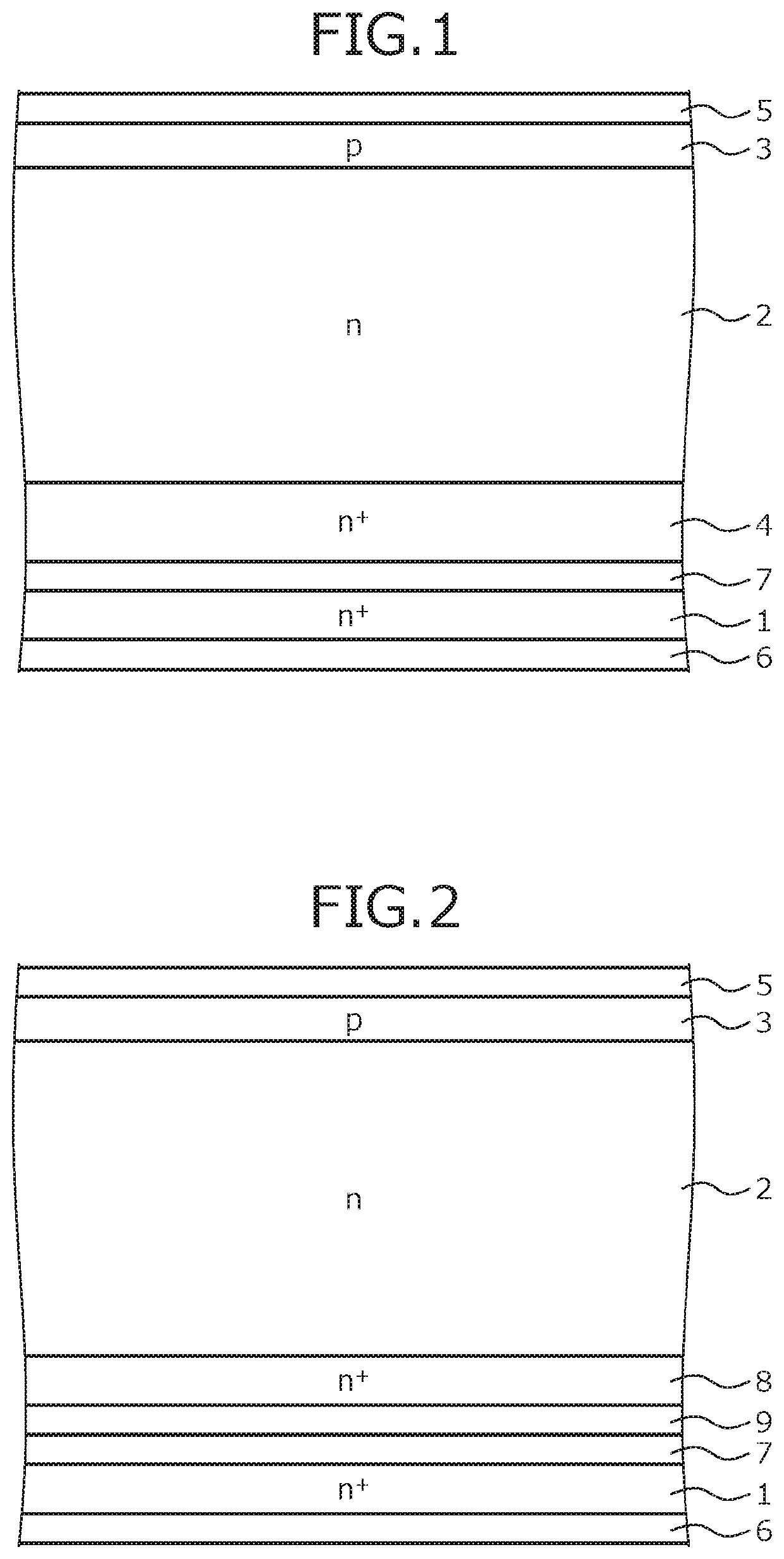
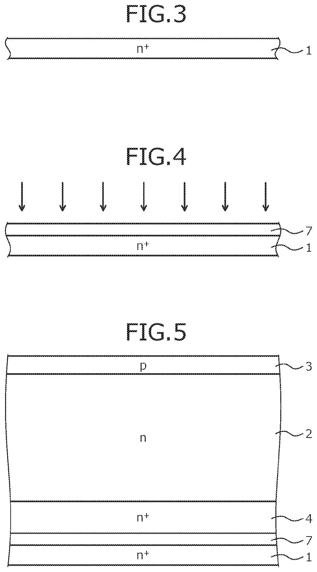
[0025]First, problems associated with the conventional techniques will be discussed. Forming the high-concentration nitrogen layer to have a uniform impurity concentration and a uniform film thickness is difficult. Furthermore, when the nitrogen concentration is too high at 2×10¹⁹ / cm3 or higher, double Shockley stacking faults (DSFs) occur. Therefore, there is a limit to suppressing the occurrence of Shockley stacking faults due to the high-concentration nitrogen layer.

[0026]Further, in the co-doped layer, after the formation of the co-doped layer, the different co-doped element may remain in a reactor (hereinafter, epi-growth reactor) of epitaxial growth equipment and management of impurities in the epi-growth reactor is difficult. This becomes particularly problematic when in the same epi-growth reactor, a drift layer of a long-lifetime such as the n-type silicon carbide layer 102 is formed successively after a buffer layer of a short-lifetime like the short-lifetime layer 104. Fu...


PUM


Abstract

A silicon carbide semiconductor device includes, sequentially, a first semiconductor layer of a first conductivity type, a second semiconductor layer of the first conductivity type provided on the first semiconductor layer, a third semiconductor layer of the first conductivity type provided on the second semiconductor layer, and a fourth semiconductor layer of a second conductivity type provided on the third semiconductor layer. A first electrode is provided on the first semiconductor layer, and a second electrode is provided on the fourth semiconductor layer. An impurity concentration of the second semiconductor layer is higher than that of the first semiconductor layer, and an impurity concentration of the third semiconductor layer is lower than that of the second semiconductor layer. The first semiconductor layer also contains, at a surface thereof in contact with the second semiconductor layer, a second impurity different from a first impurity that determines a conductivity type of the first semiconductor layer.

Description

CROSS REFERENCE TO RELATED APPLICATIONS[0001]This application is based upon and claims the benefit of priority of the prior Japanese Patent Application No. 2018-209294, filed on Nov. 6, 2018, the entire contents of which are incorporated herein by reference.BACKGROUND OF THE INVENTION1. Field of the Invention[0002]Embodiments of the invention relate to a silicon carbide semiconductor device and a method of manufacturing a silicon carbide semiconductor device.2. Description of the Related Art[0003]Conventionally, single crystal silicon has been used as a material for power semiconductor devices that control high voltage and large current. There are various types of power semiconductor devices and each is selectively used according to intended purpose. For example, P-intrinsic-N diodes (PiN diodes) and bipolar transistors as well as insulated gate bipolar transistors (IGBTs) are so-called bipolar devices. Of these devices, those handling high current density cannot switch at high spee...

Claims


Application Information

Patent Timeline
IPC IPC(8): H01L29/16H01L21/04H01L29/20
CPCH01L29/1608H01L21/046H01L29/2003H01L29/868H01L21/26506H01L29/32H01L29/861H01L29/66136H01L29/7813H01L29/1095H01L29/0623
Inventor TAWARA, TAKESHIOHSE, MINA
Owner FUJI ELECTRIC CO LTD
Why Eureka
Try Eureka