Semiconductor device

a technology of semiconductors and devices, applied in the direction of semiconductor devices, basic electric elements, electrical equipment, etc., can solve the problems of reducing affecting the performance of the device, and sometimes exceeding the maximum rating of the device,

Inactive Publication Date: 2007-02-15
KK TOSHIBA
View PDF4 Cites 6 Cited by
  • Summary
  • Abstract
  • Description
  • Claims
  • Application Information

AI Technical Summary

Benefits of technology

[0009] A semiconductor device according to an aspect of the present invention includes a base region having a first conductive type and including a channel formation region, a drain region having a second conductive type and formed to be adjacent to the base region, a drain electrode formed on a part of the drain region, a source region having the second conductive type and formed to be adjacent to the base region and be spaced from and opposed to the drain region, a gate insulation film formed on the channel formation region, another part of the drain region and a part of the source region, a gate electrode formed on the channel formation region, the other part of the drain region and the part of the source region via the gate insulation film to be opposed to them, a short electrode formed to include a top of another part of the source region, with a contact length being 0.4 μm to 0.8 μm in a part of maximum length with the source region in a direction in which the source region is opposed to the drain region, a region having the first conductive type and a higher impurity concentration than the base region, which is provided at an opposite side of the source region from a side opposed to the drain region and at an underside of the short electrode to be adjacent to the base region, a semiconductor substrate having the first conductive type and located at an underside of the region, and a source electrode formed at an underside of the semiconductor substrate.
[0010] Further, a semiconductor device according to another aspect of the present invention includes a base region having a first conductive type and including a channel formation region, a drain region having a second conductive type and formed to be adjacent to the base region, a drain electrode formed on a part of the drain region, a source region having the second conductive type and formed to be adjacent to the base region, to be spaced from and opposed to the drain region, and to be provided at intervals in a direction orthogonal to a direction opposed to the drain region, a gate insulation film formed on the channel formation region, another part of the drain region and a part of each portion of the source region, a gate electrode formed on the channel formation region, the other part of the drain region and the part of each portion of the source region via the gate insulation film to be opposed to them, a short electrode formed to include a top of another part of each portion of the source region, a region having the first conductive type and a higher impurity concentration than the base region, which is provided at an opposite side of each portion of the source region from a side opposed to the drain region and at an underside of the short electrode to be adjacent to the base region, a semiconductor substrate having the first conductive type and located at an underside of the region, and a source electrode formed at an underside of the semiconductor substrate.

Problems solved by technology

When a power field-effect transistor is used for a high-speed switching device or the like, a high surge-voltage is applied between a drain and a source at a gate turn-off timing due to an inductance of the circuit itself, and the surge voltage sometimes exceeds the maximum rating of the device and breaks the device.
However, in terms of the reduction in the number of components and the decrease in size of apparatuses, the demand to remove the serge absorbing circuit and to cause the power field-effect transistor to absorb the energy even when the surge voltage exceeds the maximum rating grows more and more.
However, such designs significantly raise the on-resistance of the device, and therefore, the performance of the device is decreased as a result.

Method used


Image

  • Semiconductor device
  • Semiconductor device
  • Semiconductor device

Examples


Embodiment Construction

Description of the Embodiments

[0021] Though embodiments of the present invention are described with reference to the drawings, but these drawings are presented only for an illustrative purpose, and in no way limit the invention.

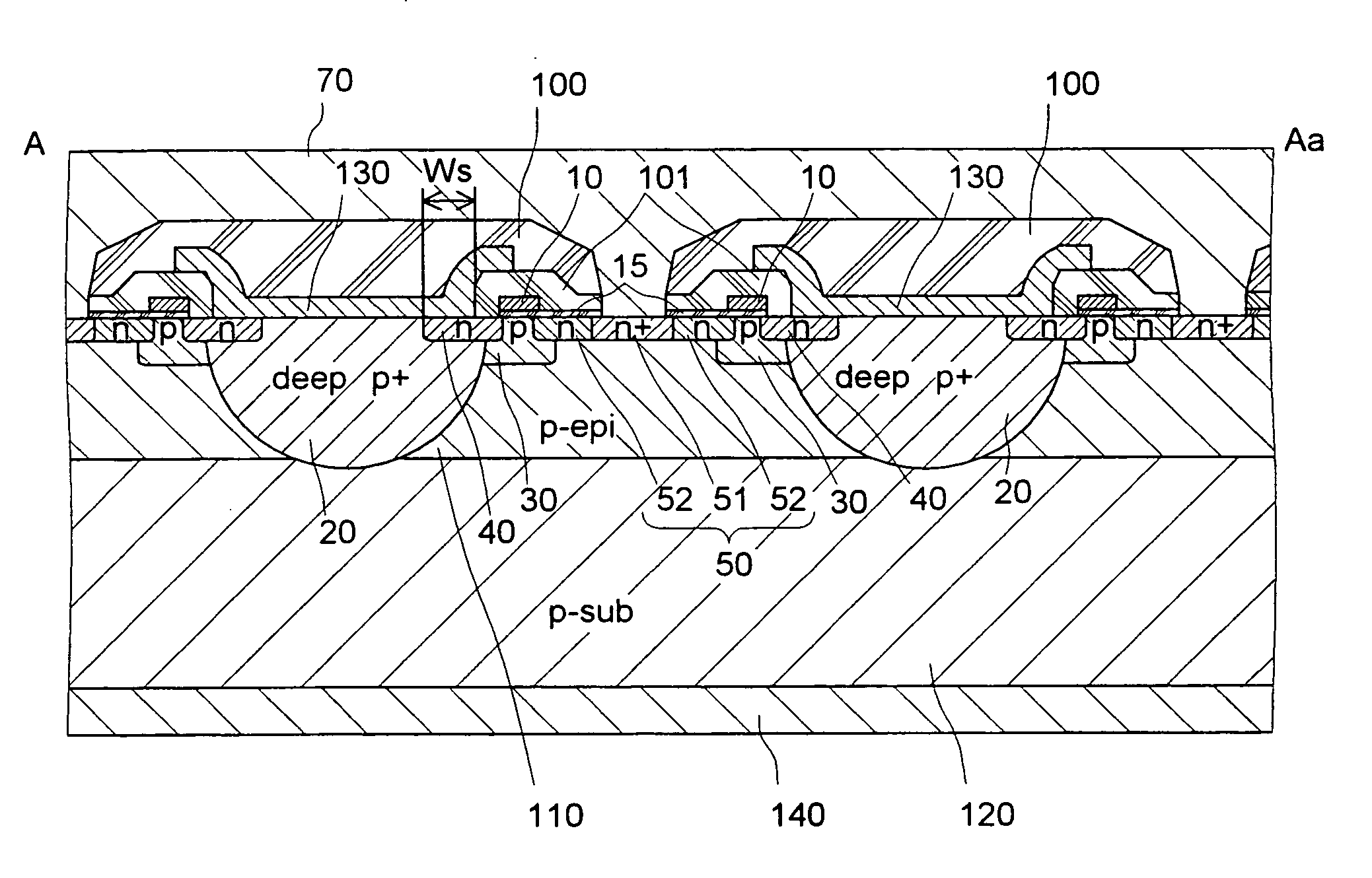
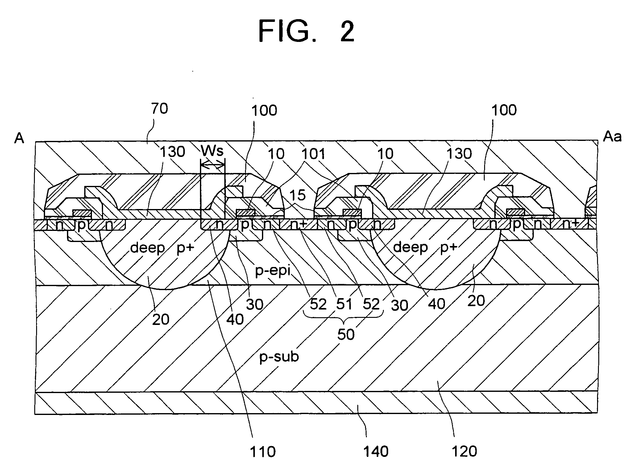
[0022] According to a semiconductor device relating to one mode of the present invention, a contact length of the short electrode (=an intermediate electrode which is electrically continuous with the source electrode) and the source region (length in a direction opposed to the drain region) is shortened to minimum limit in a range securing a necessary length, and is the length of 0.4 μm to 0.8 μm. With such a short length, the potential of the source region has less difference as compared with a potential of a base region via the short electrode and the region (high impurity concentration region). This is because the high impurity concentration region has a resistance as compared with metals though it has a high impurity concentration, and voltage drop occu...


PUM


Abstract

Disclosed is a semiconductor device including a base region having a first conductive type, a drain region and a source region having a second conductive type, a gate insulation film and a gate electrode formed on a channel formation region and on a part of the drain region and the source region, a short electrode formed to include a top of another part of the source region, with contact length being 0.4 μm to 0.8 μm in a part of maximum length with the source region in a direction in which the source region is opposed to the drain region, and a fourth region having the first conductive type and a higher impurity concentration than the base region, provided at an opposite side of the source region from a side opposed to the drain region and at an underside of the short electrode to be adjacent to the base region.

Description

CROSS-REFERENCE TO THE INVENTION [0001] This application is based upon and claims the benefit of priority from the prior Japanese Patent Application No. 2005-234081, filed on Aug. 12, 2005; the entire contents of which are incorporated herein by reference. BACKGROUND [0002] 1. Field of the Invention [0003] This invention relates to a semiconductor device for switching an electric current, and particularly to a semiconductor device preferable for an electric power use. [0004] 2. Description of the Related Art [0005] When a power field-effect transistor is used for a high-speed switching device or the like, a high surge-voltage is applied between a drain and a source at a gate turn-off timing due to an inductance of the circuit itself, and the surge voltage sometimes exceeds the maximum rating of the device and breaks the device. It is conventionally essential to protect the device by attaching a surge absorbing circuit. However, in terms of the reduction in the number of components a...

Claims


Application Information

Patent Timeline
Patent Type & Authority Applications(United States)
IPC IPC(8): H01L29/00
CPCH01L29/0696H01L29/0847H01L29/7835H01L29/4238H01L29/66659H01L29/4175
Inventor HOKOMOTO, YOSHITAKATAKANO, AKIO
Owner KK TOSHIBA
Why Eureka
Try Eureka