Electronic assembly including multiple substrates

a technology of electronic assembly and substrate, applied in the field of electronic assembly, can solve the problems of increasing the process time and cost of the assembly, and degrading the electrical performance of the electronic assembly

Active Publication Date: 2006-09-28
DELPHI TECH IP LTD
View PDF3 Cites 98 Cited by
  • Summary
  • Abstract
  • Description
  • Claims
  • Application Information

AI Technical Summary

Benefits of technology

[0004] The present invention is generally directed to an electronic assembly that includes a first substrate and a second substrate. The first substrate includes a first surface having a first plurality of conductive traces formed on an electrically non-conductive layer. The second substrate includes a first surface having a second plurality of conductive traces formed thereon and a second surface having a third plurality of conductive

Problems solved by technology

Unfortunately, the utilization of wirebonds between the substrates increases lead inductance and, as such, results in degraded electrical performance of the

Method used


Image

  • Electronic assembly including multiple substrates
  • Electronic assembly including multiple substrates
  • Electronic assembly including multiple substrates

Examples


Embodiment Construction

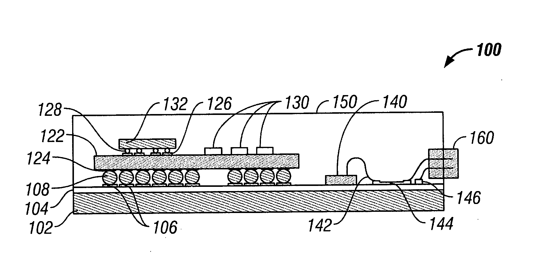
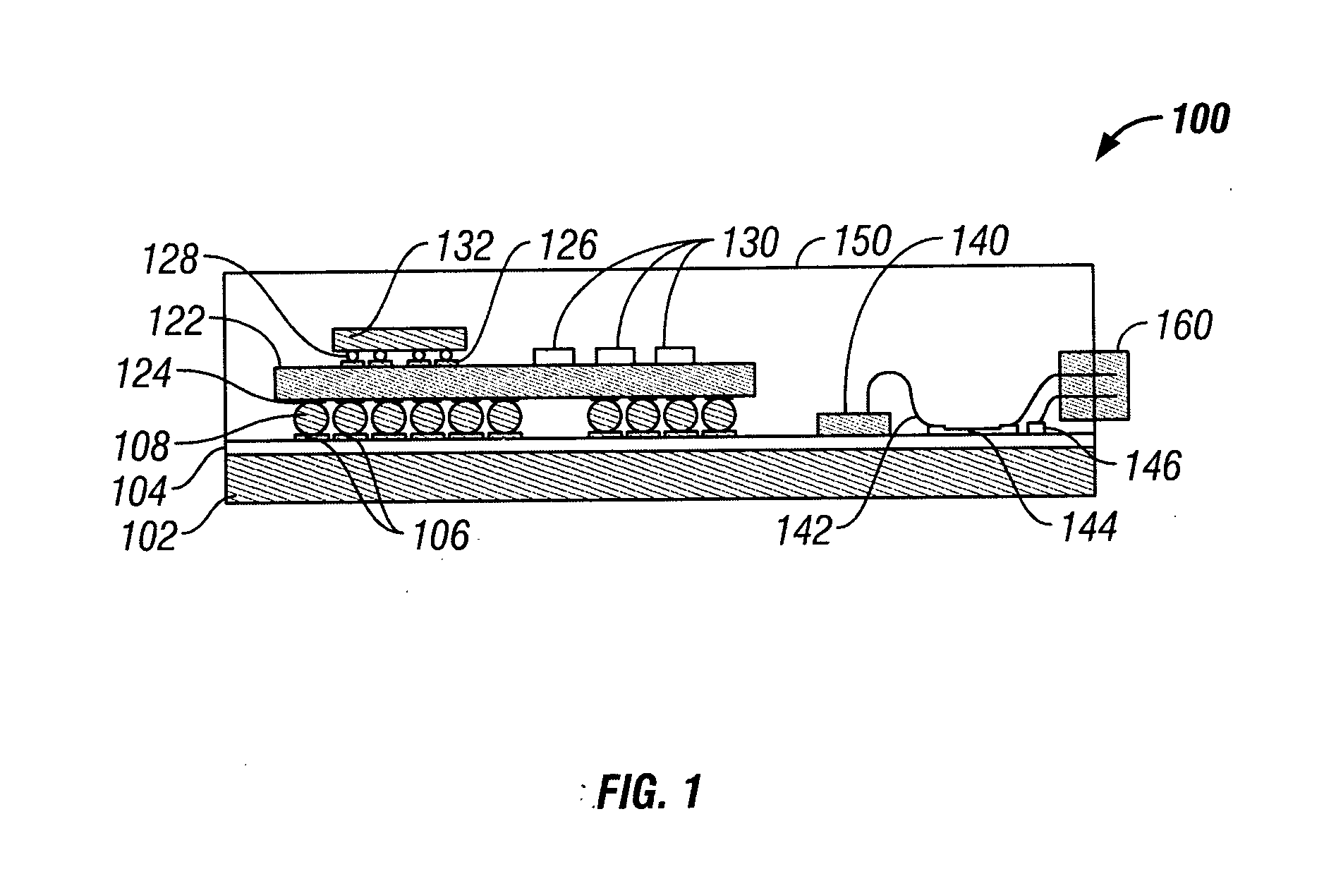
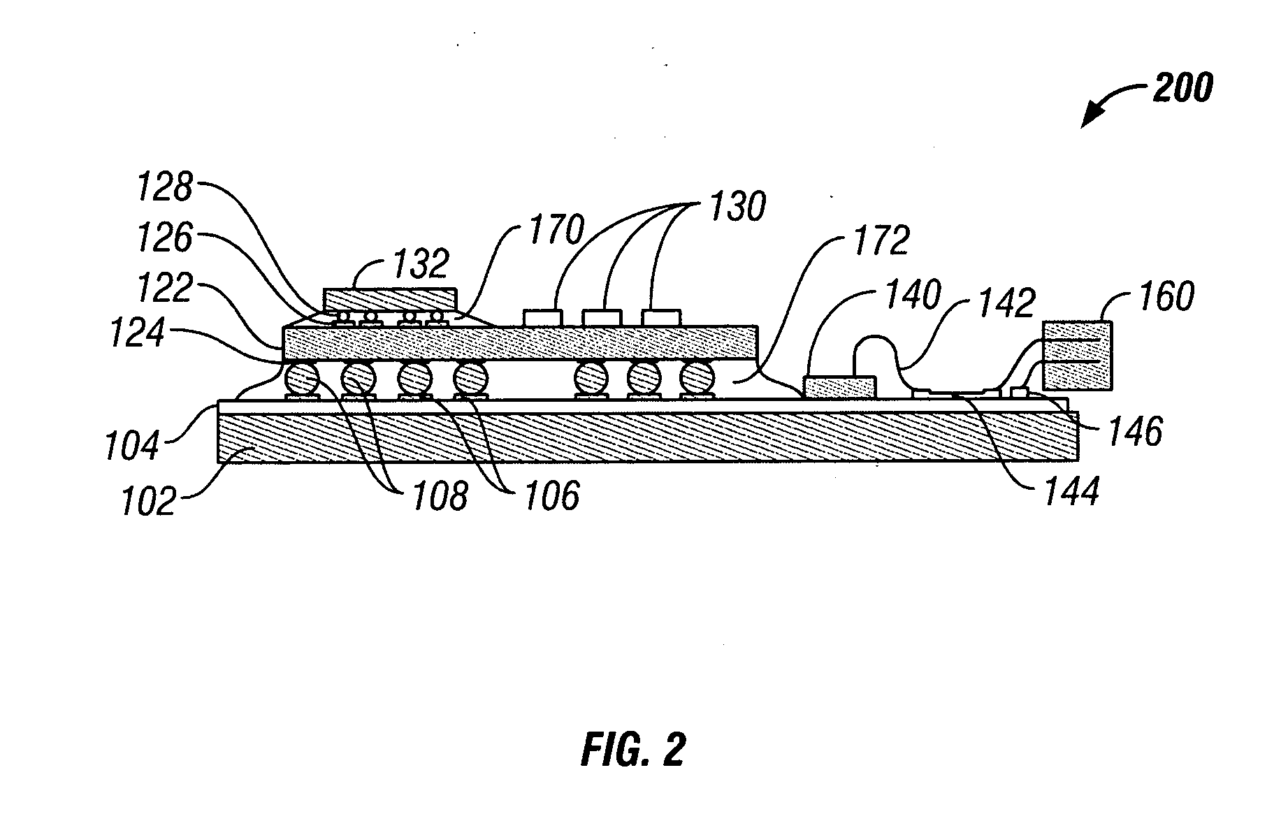
[0011] As is mentioned above, a variety of different design solutions have been proposed to improve the thermal capability of electronic assemblies that have utilized substrates, e.g., low-temperature co-fired ceramic (LTCC) substrates, that exhibit relatively low thermal conductivity in high-power applications. As is noted above, one such prior art electronic assembly offers a two substrate solution that requires wirebonds between the substrates and an adhesive bond in a primary thermal path of the electronic assembly. According to the present invention, a number of different packaging technologies are utilized to create a two substrate approach for high-power applications.

[0012] In one electronic assembly, an LTCC substrate and a stainless steel substrate are utilized. In this assembly, a high-density LTCC substrate is attached to an insulated stainless steel substrate in a manner similar to how surface mount components are mounted to a substrate. This eliminates the need for wir...


PUM


Abstract

An electronic assembly includes a first substrate and a second substrate. The first substrate includes a first surface having a first plurality of conductive traces formed on an electrically non-conductive layer. The second substrate includes a first surface having a second plurality of conductive traces formed thereon and a second surface having a third plurality of conductive traces formed thereon. A first electronic component is electrically coupled to one or more of the plurality of conductive traces on the first surface of the second substrate. At least one of a plurality of conductive interconnects is incorporated within each solder joint that electrically couples one or more of the conductive traces formed on the second surface of the second substrate to one or more of the conductive traces formed on the first substrate.

Description

TECHNICAL FIELD [0001] The present invention is generally directed to an electronic assembly and, more specifically, to an electronic assembly including multiple substrates. BACKGROUND OF THE INVENTION [0002] Various manufacturers have offered electronic assemblies including multiple substrates, at least one of which has been a low-temperature co-fired ceramic (LTCC) substrate. In general, LTCC substrates allow for electronic assemblies that have relatively high-density circuitry. However, in electronic assemblies that have incorporated an LTCC substrate, it is often desirable to configure the assembly to improve the thermal conductivity of the LTCC substrate, as LTCC substrates have a relatively low thermal conductivity of approximately 3Wm / K. This is particularly desirable when LTCC substrates are utilized in high-power applications. In at least one prior art electronic assembly that utilizes multiple substrates, an LTCC substrate has been wirebonded to another substrate. In this ...

Claims


Application Information

Patent Timeline
IPC IPC(8): H01L23/52
CPCH01L21/563H01L23/142H01L2924/1305H01L2924/30107H01L2924/15311H01L2224/73204H01L2224/48227H01L2224/32225H01L2224/16225H05K2201/10977H05K2201/0212H05K3/3436H05K3/284H05K1/141H01L23/5385H01L2924/09701H01L2924/13055H05K1/0306H05K1/053H01L2924/00H01L2924/00011H01L2924/00014H01L2224/0401
Inventor FAIRCHILD, M. RAYSARMA, DWADASI H.R.WORKMAN, DEREK B.HARSHBARGER, DANIEL R.
Owner DELPHI TECH IP LTD
Why Eureka
Try Eureka