System and method for increasing wiring channels/density under dense via fields

a technology of dense via fields and wiring channels, which is applied in the direction of printed circuit manufacturing, printed circuit aspects, computer aided design, etc., can solve the problems of reducing the yield, increasing the base cost of printed circuit boards, and increasing costs, so as to increase the wiring channels/densities and maximize signal line wiring

Inactive Publication Date: 2006-10-05
IBM CORP
View PDF11 Cites 7 Cited by
  • Summary
  • Abstract
  • Description
  • Claims
  • Application Information

AI Technical Summary

Benefits of technology

[0009] The present invention provides a system and method for increasing the wiring channels / density under dense via fields of a circuit board. With the system and method of the present invention, a channel of power / ground lines is identified with the power / ground line surface pads and associated plated through holes or vias identified as candidates for removal of the plated through holes or vias beneath the surface pads. In an exemplary embodiment, the power / ground lines for the circuit board whose vias are removed are designed to be provided in an orthogonal or diagonal pattern in order to provide channel through which additional signal lines may be routed. Thus, with these power / ground lines, contact is provided only with a surface pad (no vias are present under these surface pads). Therefore, the land grid array (LGA) / ball grid array (BGA) makes contact only on the surface pads of the printed circuit board instead of through vias underneath these surface pads. This opens up wiring channels, which previously used to be occupied by plated through holes and anti-pads, which can now be used for maximizing signal line wiring.

Problems solved by technology

However, adding additional layers to the circuit board increases the base cost of the printed circuit board.
Other solutions use thinner wiring to escape under the module which detracts from the yield and increases the cost.

Method used


Image

  • System and method for increasing wiring channels/density under dense via fields
  • System and method for increasing wiring channels/density under dense via fields
  • System and method for increasing wiring channels/density under dense via fields

Examples


Embodiment Construction

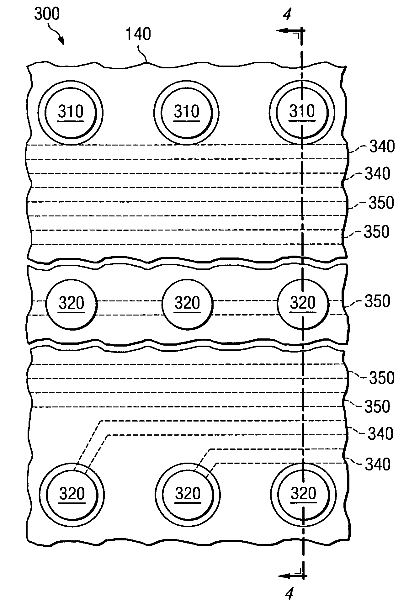
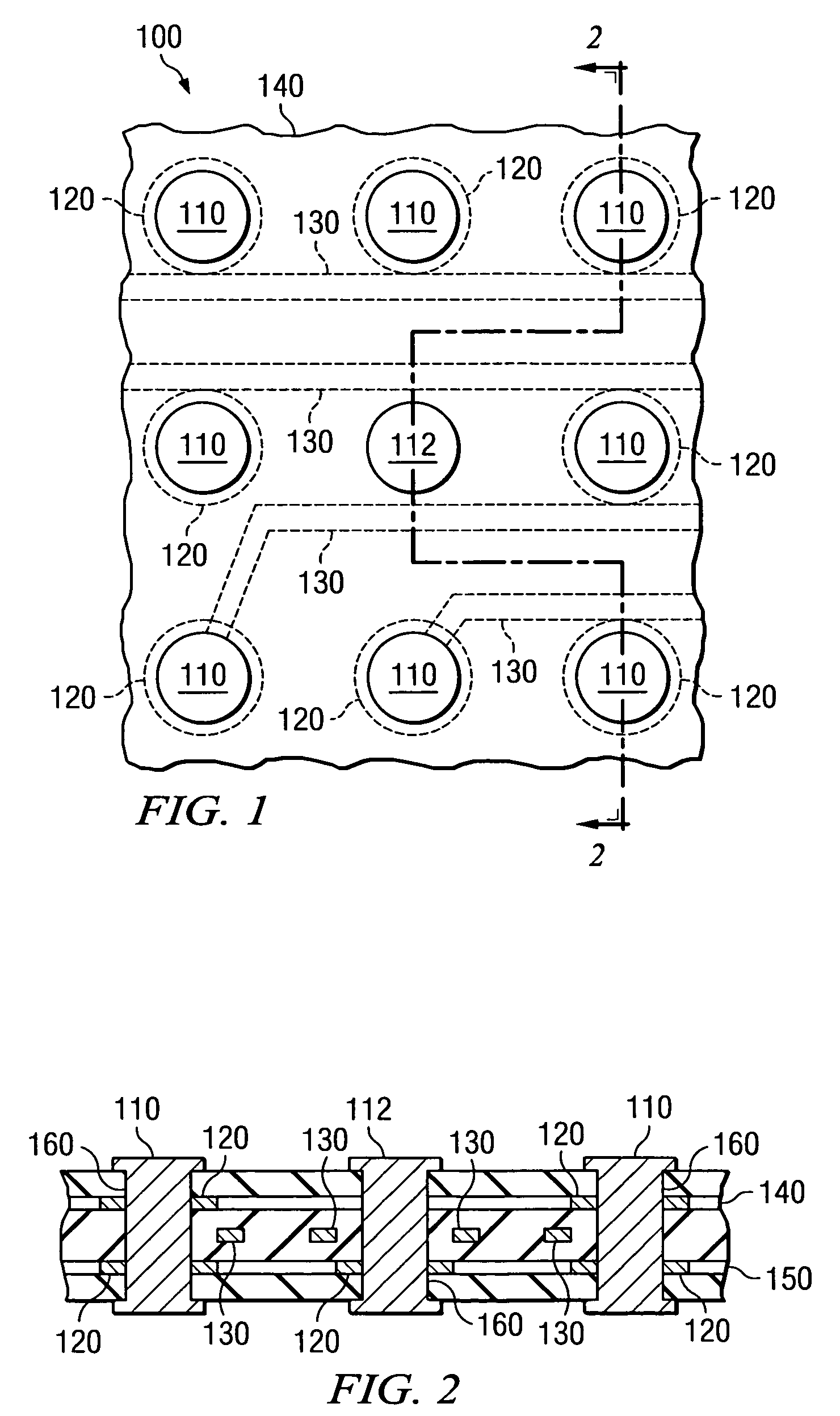
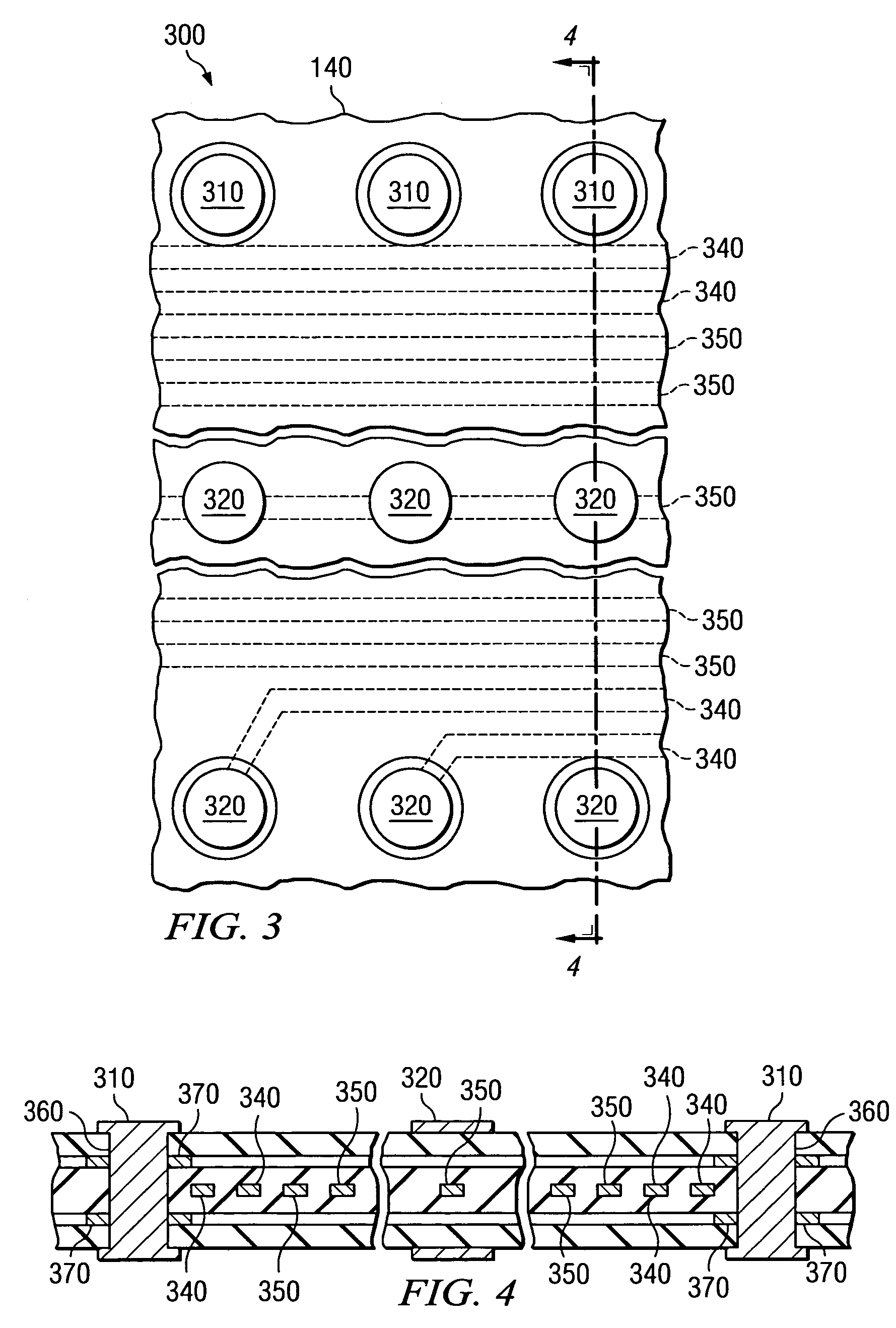
[0020]FIG. 1 is an exemplary top view of a portion of an area array of a circuit board in accordance with a known structure. As shown in FIG. 1, the area array 100 includes a plurality of surface pads 110, anti-pads 120, and signal wires 130. The anti-pads 120 isolate the plated through holes, or vias, under the surface pads 110 from the power / ground wirings on respective ones of the planes of the printed circuit board. As shown in FIG. 1, the plated through holes under all of the surface pads 110 except surface pad 112 have anti-pads 120 that isolate them from the power / ground wirings on plane 140. The power / ground wiring on the plane 140 is coupled to the plated through hole under surface pad 112.

[0021]FIG. 2 is a cross-sectional view of the portion of the area array of the circuit board shown in FIG. 1. As shown in FIG. 2, under each surface pad 110 is a plated through hole 160 that passes through layers / planes 140 and 150 of the printed circuit board. Although FIG. 2 only shows...


PUM

PropertyMeasurementUnit
diameteraaaaaaaaaa
diameteraaaaaaaaaa
areaaaaaaaaaaa

Abstract

A system and method for increasing the wiring channels/density under dense via fields of a circuit board are provided. With the system and method, the power/ground lines for the circuit board are designed to be provided in an orthogonal or diagonal pattern. The land grid array (LGA)/ball grid array (BGA) makes contact only on the surface pads of the printed circuit board with no plated through holes/vias underneath these surface pads. This opens up wiring channels, which previously used to be occupied by plated through holes and anti-pads, that can now be used for maximizing signal line wiring routing.

Description

BACKGROUND OF THE INVENTION [0001] 1. Technical Field [0002] The present invention is generally directed to an improved integrated circuit design. More specifically, the present invention is directed to a system and method for increasing wiring channels / density under dense via fields of integrated circuits of a computer card. [0003] 2. Description of Related Art [0004] Current printed circuit board constructions require one or more external conductive layers, e.g., circuitry and / or pads for mounting components thereon, and, given today's increased functional demands, a plurality of internal conductive planes, e.g., signal, power and / or ground. To provide effective interconnections between components and the board's conductive circuitry and pads, the use of through holes has been adopted wherein several such holes are passed through the board and electrically coupled in a selective manner to internal and external conductive elements. Such holes typically include a conductive, e.g., c...

Claims


Application Information

Patent Timeline
Patent Type & Authority Applications(United States)
IPC IPC(8): H05K7/06
CPCG06F17/5077H01L21/486H01L23/49822H01L23/49838H05K1/111H05K1/112Y10T29/49156H05K3/429H05K2201/09227H05K2201/10734H01L2924/0002H05K3/0005H01L2924/00G06F30/394
Inventor HARIDASS, ANANDKALLER, DIERKKLINK, ERICHTHOMKE, GISBERT GERHARD
Owner IBM CORP
Why Eureka
Try Eureka