Printed circuit board (PCB) with electrostatic discharge protection

a printed circuit board and electrostatic discharge technology, which is applied in the direction of electrostatic discharge protection, overvoltage arrestors using spark gaps, metallic pattern materials, etc., can solve the problems of inability to continue normal operation of integrated circuits with overstressed elements, inability to accumulate electrostatic charges and resulting destruction upon the elements, and permanent destruction or unstable operation of semiconductor elements

Inactive Publication Date: 2006-11-30
BENQ CORP
View PDF7 Cites 18 Cited by
  • Summary
  • Abstract
  • Description
  • Claims
  • Application Information

AI Technical Summary

Problems solved by technology

The destroy from overstressing may lead to permanent destruction or unstable operation to the semiconductor elements.
As a clear consequence, an integrated circuit having overstressed elements may have difficulty to continue its normal operation.
Also, the accumulation of the electrostatic charges as well as the resulting destruction upon the elements are implicit and, definitely, not easy to be located.
In a compact or small-size electronic product such as a cellular phon

Method used


Image

  • Printed circuit board (PCB) with electrostatic discharge protection
  • Printed circuit board (PCB) with electrostatic discharge protection
  • Printed circuit board (PCB) with electrostatic discharge protection

Examples


Embodiment Construction

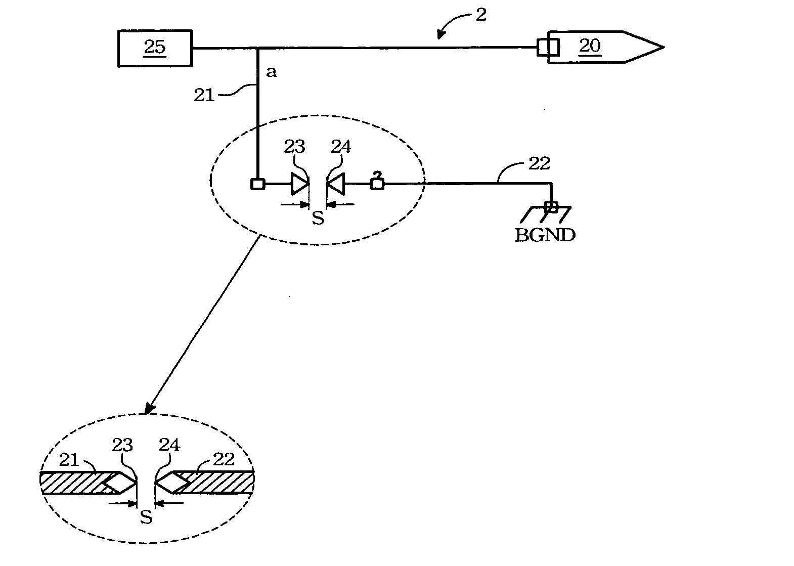
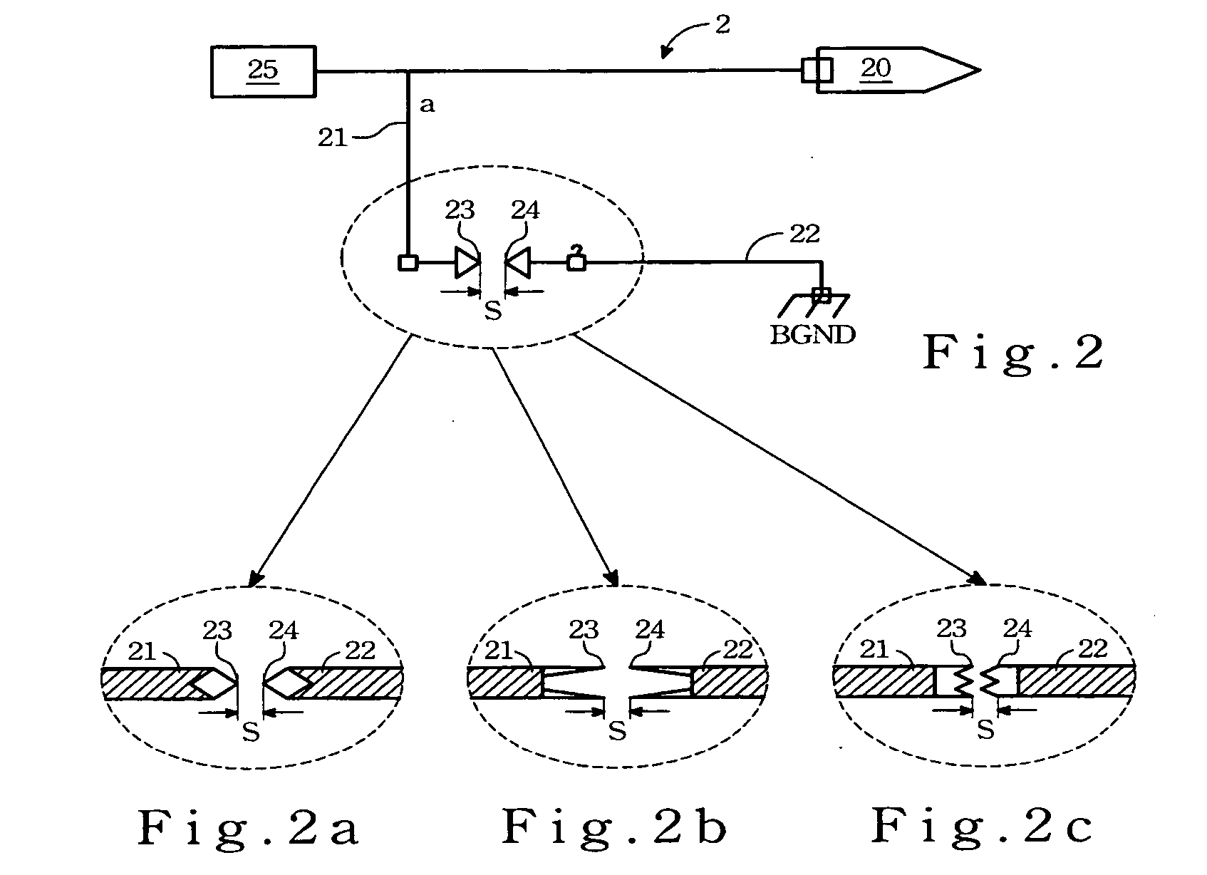
[0017] This invention uses a layout edge with an exposed copper on the printed circuit board to carry out the point discharge principle.

[0018] Referring to FIG. 2, a printed circuit board with electrostatic discharge protection includes an internal element 20, a lead wire 21, a ground wire 22, a first edge 23, a second edge 24 ,and a terminal 25. On the printed circuit board 2, the internal element 20 is connected with the terminal 25, and the lead wire 21 is connected to the wire that connects the element 20 and the terminal 25. The lead wire 21 is extended to form the first edge 23 with an exposed copper. Further, corresponds to the first edge 23, the second edge 24 with an exposed copper is formed to further connect to the ground wire 22. If the printed circuit board 2 is designed to be a multiplayer PCB, a throughhole in the PCB can be constructed to establish wire connection to a ground level. By providing the pair of the first edges 23 and the second edges 24, electrostatic d...


PUM


Abstract

A printed circuit board (PCB) with electrostatic discharge protection includes at least a lead wire having a first edge with an exposed copper, and a ground wire having a second edge with another exposed copper, in which the first edge faces the second edge with a predetermined spacing. By providing the pair of the first and the second edges, electrostatic discharge of the PCB can be arbitrarily carried out between the lead wire and the ground wire.

Description

FIELD OF THE INVENTION [0001] The present invention relates to a printed circuit board (PCB) with electrostatic discharge protection, more particularly to the PCB having an edge with an exposed copper for providing the electrostatic discharge function to the PCB. BACKGROUND OF THE INVENTION [0002] The electrostatic discharge (ESD) is defined that an accumulated electrostatic charge is discharged from a high electrostatic charge collection area to an opposite electric charge collection area or a low electric charge collection area. Also, the electrostatic discharge is known in the art as one of primary destroy factors, which cause majority electronic components or the electronic system to be electrically overstressed. The destroy from overstressing may lead to permanent destruction or unstable operation to the semiconductor elements. As a clear consequence, an integrated circuit having overstressed elements may have difficulty to continue its normal operation. Also, the accumulation ...

Claims


Application Information

Patent Timeline
IPC IPC(8): H05K1/11H05K1/09
CPCH01T4/08H05K9/0067H05K1/026
Inventor TUNG, CHIA-HSINLIN, JIMLIU, CHI-WEILEE, HOW-PING
Owner BENQ CORP
Why Eureka
Try Eureka