Integrated circuit package having stacked integrated circuits and method therefor

a technology of integrated circuits and integrated circuits, which is applied in the direction of electrical equipment, semiconductor devices, semiconductor/solid-state device details, etc., can solve the problems of increasing the overall height and thickening the thickness of the integrated circuit package. achieve the effect of reducing the number of process steps and increasing the stacking density of the integrated circuit di

Inactive Publication Date: 2006-11-30
SANDISK TECH LLC
View PDF53 Cites 129 Cited by
  • Summary
  • Abstract
  • Description
  • Claims
  • Application Information

AI Technical Summary

Benefits of technology

[0008] Broadly speaking, the invention provides improved techniques for stacking integrated circuit dies within an integrated circuit package. These improved techniques allow greater stacking density of integrated circuit dies within an integrated circuit package. Additionally, the improved stacking techniques permit conventional bonding techniques for electrical connection of the various integrated circuit dies to each other or to a substrate. Still further, the improved stacking techniques substantially reduce the number of process steps required to fabricate integrated circuit packages having a plurality of stacked integrated circuit dies.

Problems solved by technology

Although the spacer provides the lower die with sufficient space so that it can be wire bonded, the spacer disadvantageously makes the integrated circuit package thicker or limits the number of dies that can fit within the integrated circuit package of a given size.
Unfortunately, however, the spacer die 108 increases the overall height of the integrated circuit package 100.

Method used


Image

  • Integrated circuit package having stacked integrated circuits and method therefor
  • Integrated circuit package having stacked integrated circuits and method therefor
  • Integrated circuit package having stacked integrated circuits and method therefor

Examples


Embodiment Construction

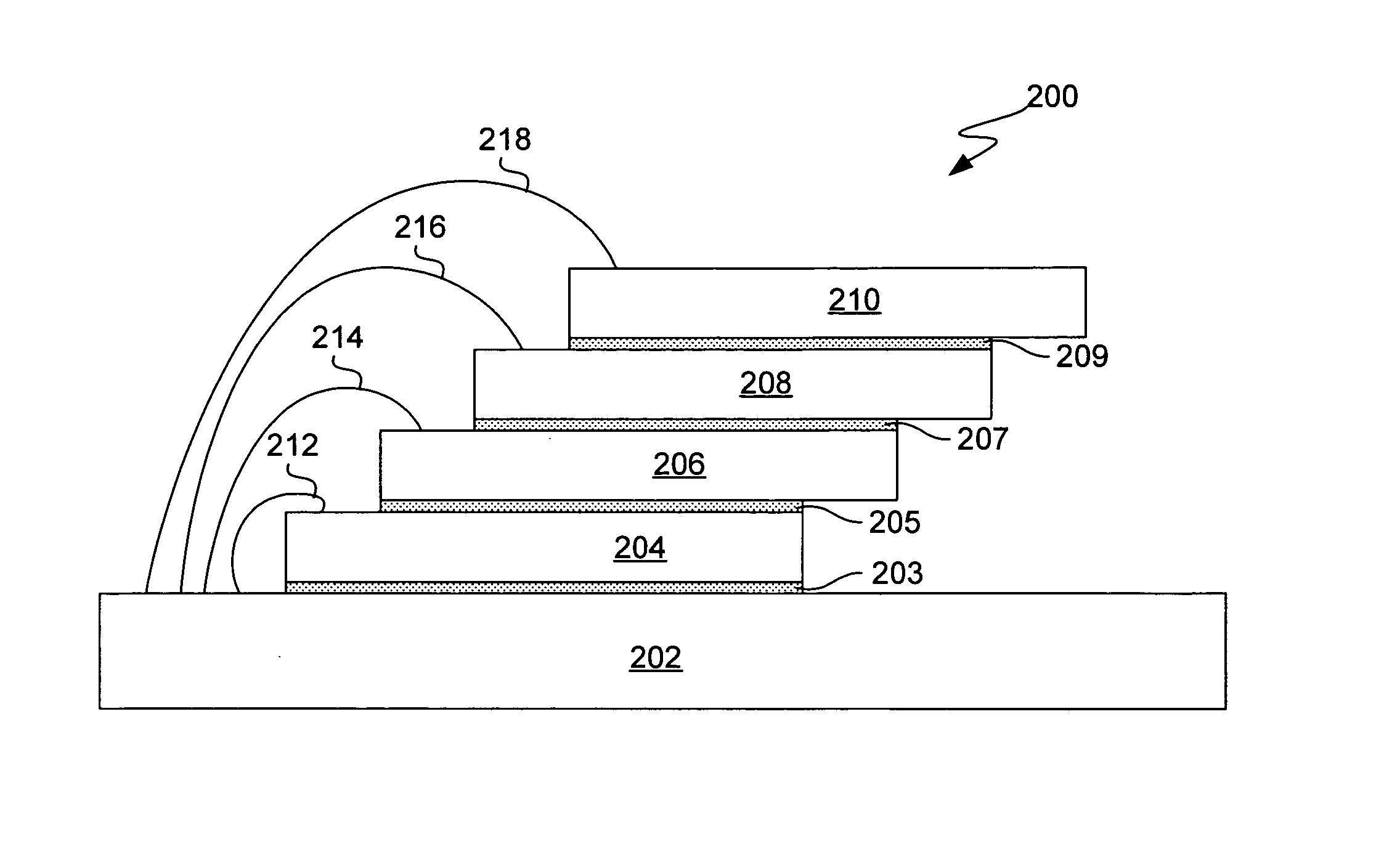
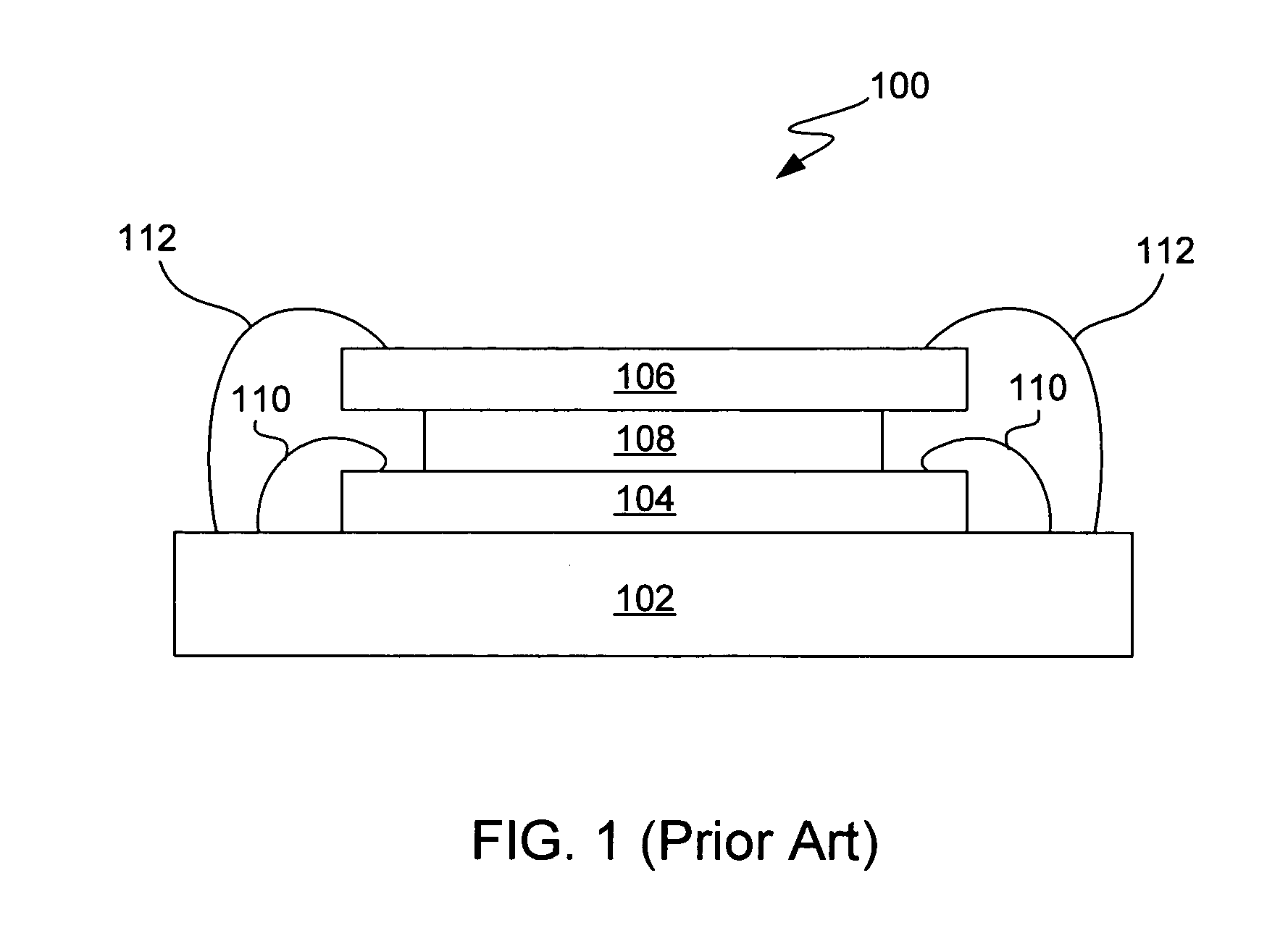
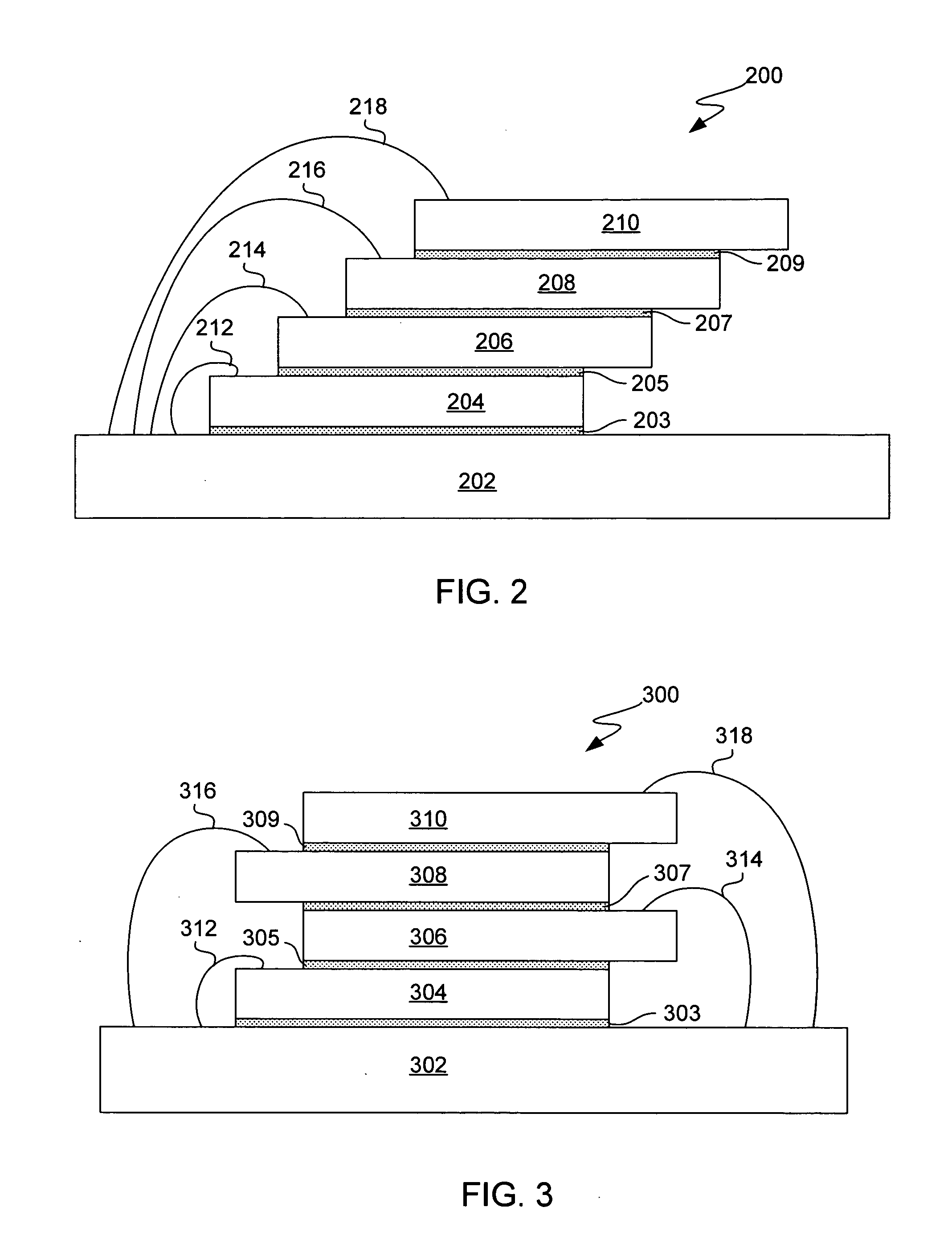
[0027] The invention provides improved techniques for stacking integrated circuit dies within an integrated circuit package. These improved techniques allow greater stacking density of integrated circuit dies within an integrated circuit package. Additionally, the improved stacking techniques permit conventional bonding techniques for electrical connection of the various integrated circuit dies to each other or to a substrate. Still further, the improved stacking techniques substantially reduce the number of process steps required to fabricate integrated circuit packages having a plurality of stacked integrated circuit dies.

[0028] These techniques are particularly useful for integrated circuit packages that are thin or low profile because the resulting integrated circuit packages can provided greater utility (i.e., greater functional ability or greater capacity). These improved approaches are also particularly useful for stacking same size (and often same function) integrated circu...


PUM


Abstract

Improved techniques for stacking integrated circuit dies within an integrated circuit package are disclosed. These improved techniques allow greater stacking density of integrated circuit dies within an integrated circuit package. Additionally, the improved stacking techniques permit conventional bonding techniques for electrical connection of the various integrated circuit dies to each other or to a substrate. These improved approaches are particularly useful for stacking same size (and often same function) integrated circuit dies within integrated circuit packages. One example of such an integrated circuit package is a non-volatile memory integrated circuit package that contains multiple, like-sized memory storage integrated circuit dies arranged in a stack.

Description

CROSS-REFERENCE TO RELATED APPLICATIONS [0001] This application is related to U.S. patent application Ser. No. 10 / 463,742 (Aft. Dkt. No.: SDK1P016 / 446), filed Jun. 16, 2003, and entitled “INTEGRATED CIRCUIT PACKAGE HAVING STACKED INTEGRATED CIRCUITS AND METHOD THEREFOR”, and which is hereby incorporated by reference herein. This application is also related to U.S. patent application Ser. No. 10 / 463,051 (Att. Dkt. No.: SDK1P013 / 369), filed Jun. 16, 2003, and entitled “STACKABLE INTEGRATED CIRCUIT PACKAGE AND METHOD THEREFOR”, and which is hereby incorporated by reference herein.BACKGROUND OF THE INVENTION [0002] 1. Field of the Invention [0003] The present invention relates to integrated circuit packages and, more particularly, to integrated circuit packages that include stacked integrated circuits. [0004] 2. Description of the Related Art [0005] As the trend for memory integrated circuit (IC) packages to be smaller and their memory density to be larger continues, advancements in pac...

Claims


Application Information

Patent Timeline
Patent Type & Authority Applications(United States)
IPC IPC(8): H01L23/02
CPCH01L25/0657H01L2224/32145H01L2224/73265H01L2224/48227H01L2224/48145H01L2224/32225H01L2224/16225H01L2924/01004H01L2225/06562H01L2224/48147H01L2224/48091H01L2924/00014H01L2924/00012H01L24/73H01L2924/14H01L2924/00H01L23/12
Inventor TAKIAR, HEM P.BHAGATH, SHRIKARMING WANG, KEN JIAN
Owner SANDISK TECH LLC
Why Eureka
Try Eureka