FinFET split gate EEPROM structure and method of its fabrication

a technology of finfet and split gate, which is applied in the direction of semiconductor devices, electrical equipment, transistors, etc., can solve the problems of affecting the ability of the gate to turn the device, affecting the ability of the gate to operate appropriately, and complex and expensive prior techniques for fabricating fet eeproms

Active Publication Date: 2006-12-14
TAIWAN SEMICON MFG CO LTD
View PDF5 Cites 249 Cited by
  • Summary
  • Abstract
  • Description
  • Claims
  • Application Information

AI Technical Summary

Benefits of technology

[0014] In preferred embodiments, the insulative strata are portions of an insulative overlayer that covers the stack, the portions of the fin (including the second channel portion) not covered by the stack, and portions of the insulative layer not covered by the stack and the fin. The first insulative

Problems solved by technology

Prior techniques for fabricating FET EEPROMs are complicated and costly and often produce memories that do not operate appropriately, as noted in the '836 patent.
However, as FETs are scaled to possess channel lengths less than 100 nm, their conventional stacked or horizontal orientation may lead to several problems,

Method used


Image

  • FinFET split gate EEPROM structure and method of its fabrication
  • FinFET split gate EEPROM structure and method of its fabrication
  • FinFET split gate EEPROM structure and method of its fabrication

Examples


Embodiment Construction

[0023] The Figures referred to herein are not to scale. The relative dimensions of the various elements depicted in the drawings are not intended to represent the actual dimensional proportionality of these elements, but are, rather, merely intended to clearly set forth for the benefit of those having ordinary skill in the art how to make and use, as well as the inventive concepts underlying, the present invention.

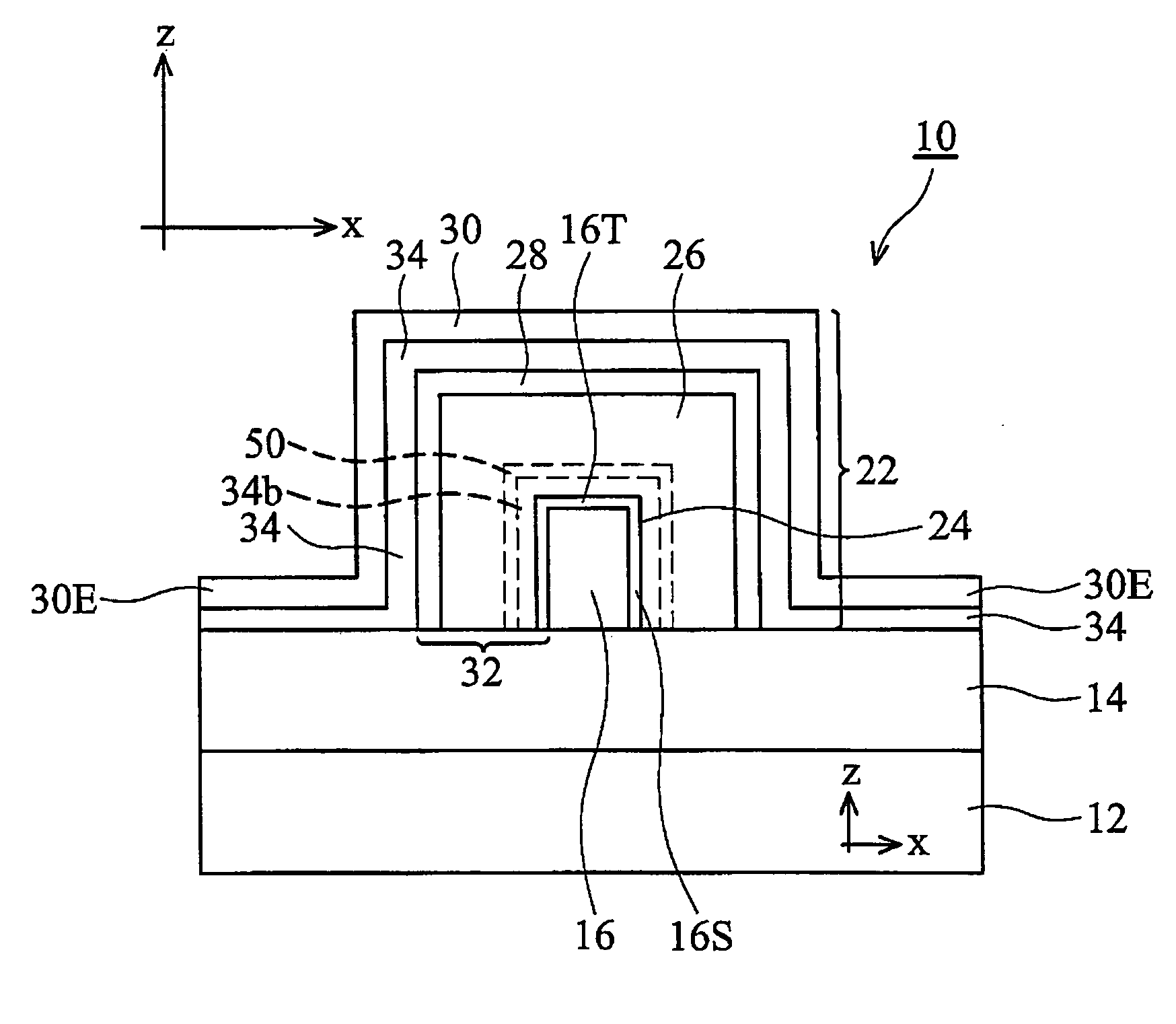
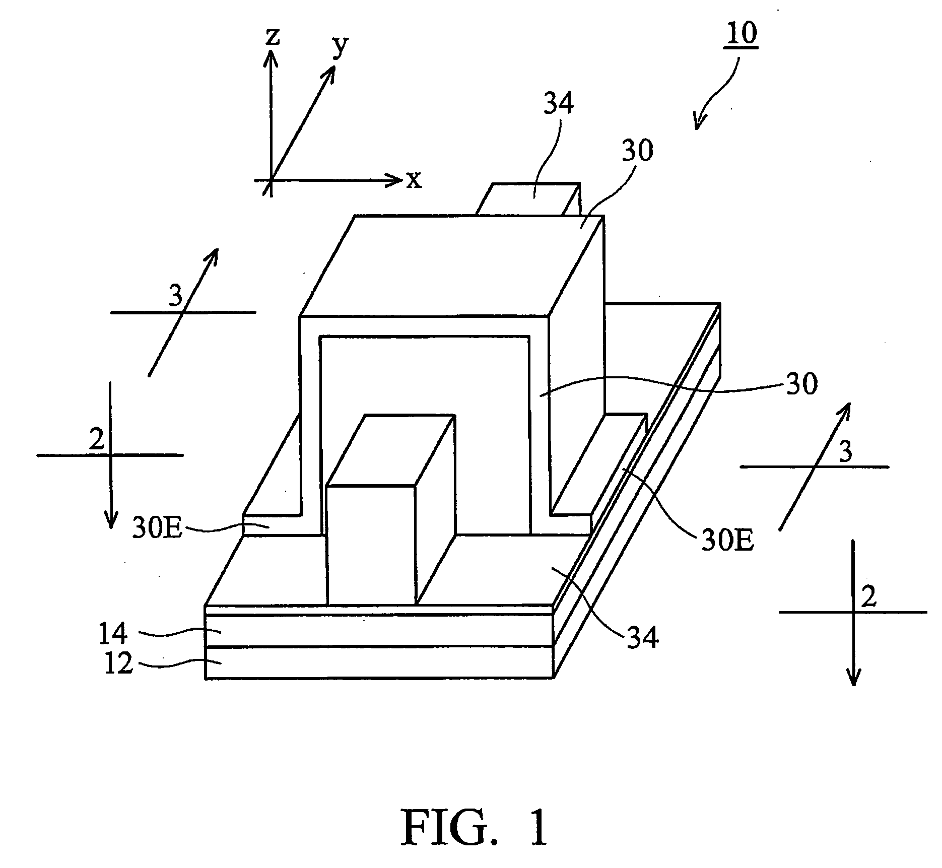
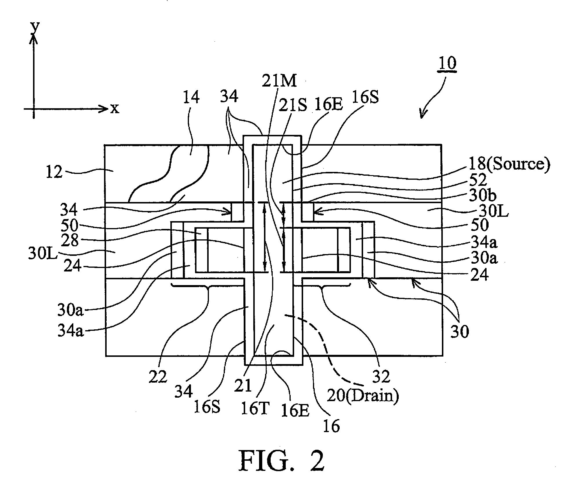
[0024] Referring first to FIGS. 1-4, and particularly to FIGS. 2 and 3, there is generally shown an embodiment of a split gate FinFET EEPROM structure 10 as contemplated by the present invention. The structure 10 is preferably fabricated according to conventional deposit / form-and-etch / remove CMOS protocols. The split gate FinFET EEPROM 10 is preferably an SOI structure, although bulk procedures are also contemplated.

[0025] The structure 10 includes a generally planar semiconductor substrate 12, for example of silicon, on which there is formed or deposited an insulative f...


PUM


Abstract

A FinFET split gate EEPROM structure includes a semiconductor substrate and an elongated semiconductor fin extending above the substrate. A control gate straddles the fin, the fin's sides and a first drain-proximate portion of a channel between a source and drain in the fin. The control gate includes a tunnel layer and a floating electrode over which are a first insulative stratum and a first conductive stratum. A select gate straddles the fin and its sides and a second, source-promixate portion of the channel. The select gate includes a second insulative stratum and a second conductive stratum. The insulative strata are portions of a continuous insulative layer covering the substrate and the fin. The conductive strata are electrically continuous portions of a continuous conductive layer formed on the insulative layer.

Description

TECHNICAL FIELD [0001] The present invention relates to a split gate FinFET EEPROM structure and to a method of fabricating the structure. More specifically, the embodiments of the present invention combine FinFET technology and split gate EEPROM technology to obtain the benefits of both technologies in a single flash memory structure. Other embodiments of the invention relate to methods for fabricating the foregoing flash memory structure. BACKGROUND [0002] Numerous conventional techniques exist for fabricating transistors, such as FETs, and integrated circuits containing FETs. See commonly assigned U.S. Pat. No. 6,465,836 and prior art referred to therein (the “'836 patent”). Similarly, there exist numerous conventional IC techniques for fabricating non-volatile, erasable memories, such as EEPROMs (“flash memories”), the data storage and transduction capabilities of which are not based on transient operation, as is the case with bipolar junction transistors. Moreover, the fabricat...

Claims


Application Information

Patent Timeline
IPC IPC(8): H01L29/788H01L21/336
CPCH01L21/28273H01L29/42328H01L29/7881H01L29/66825H01L29/785H01L29/66795H01L29/40114
Inventor LEE, DI-HONGTSAO, HSUN-CHIHCHEN, KUANG-HSINCHEN, HUNG-WEI
Owner TAIWAN SEMICON MFG CO LTD
Why Eureka
Try Eureka