Multilayer chip capacitor

a multi-layer chip and capacitor technology, applied in the direction of fixed capacitors, stacked capacitors, fixed capacitor details, etc., can solve the problem of hard to reduce esl sufficiently, and achieve the effect of preventing mutual inductance, reducing esl, and reducing magnetic flux

Inactive Publication Date: 2006-12-21
SAMSUNG ELECTRO MECHANICS CO LTD
View PDF9 Cites 12 Cited by
  • Summary
  • Abstract
  • Description
  • Claims
  • Application Information

AI Technical Summary

Benefits of technology

[0019] According to the invention, vertically adjacent ones of the leads having the same polarity extend in different directions at a predetermined angle. Therefore, currents flow through the leads in different directions. This minimizes increase in magnetic flux and prevents mutual inductance from occurring as in the prior art. Consequently, the multilayer chip capacitor has much lower ESL.

Problems solved by technology

This mutual inductance renders it hard to reduce ESL sufficiently.

Method used


Image

  • Multilayer chip capacitor
  • Multilayer chip capacitor
  • Multilayer chip capacitor

Examples


first embodiment

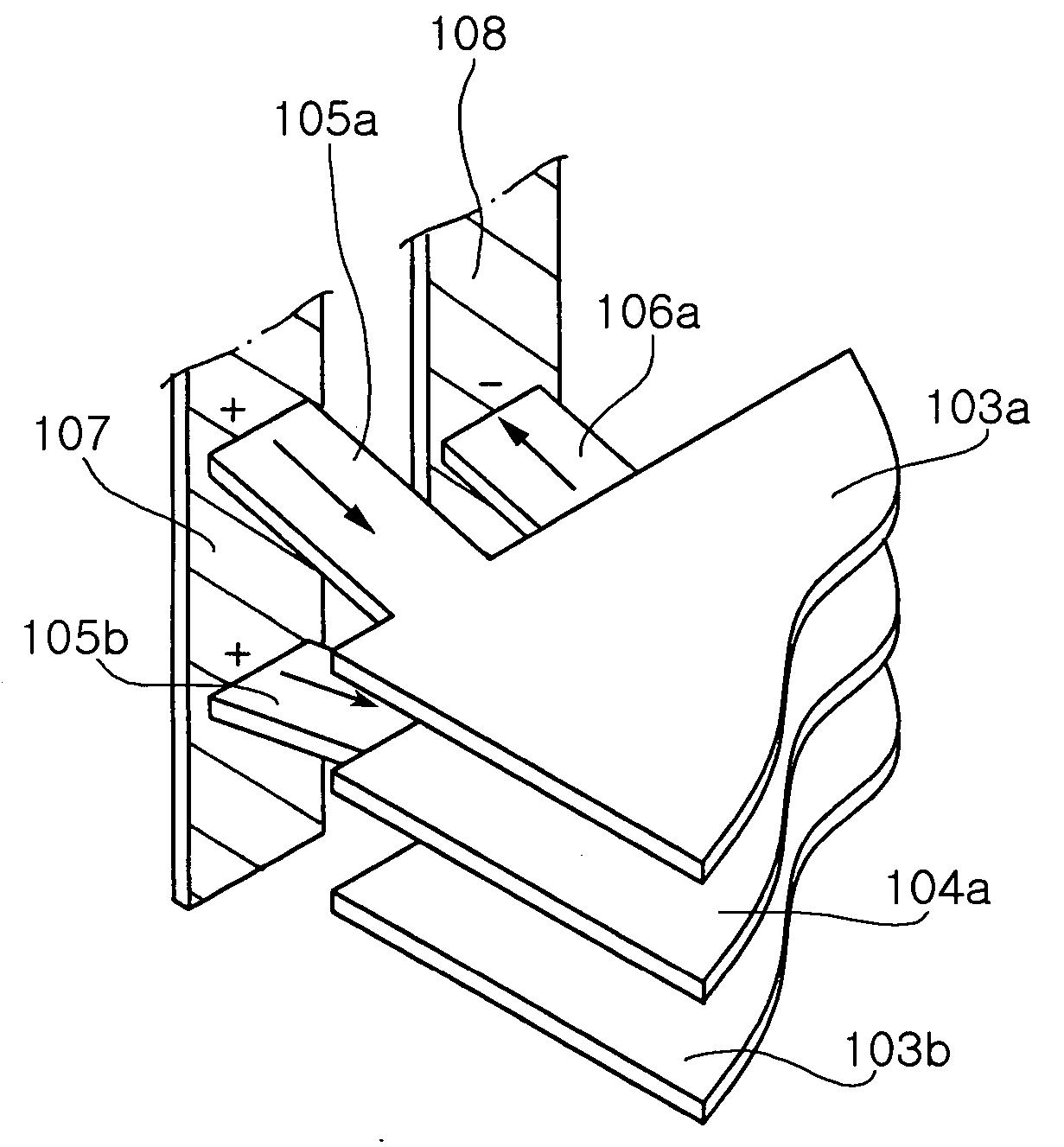
[0050]FIGS. 7a and 7b are plan views illustrating internal electrodes of the capacitor according to the invention. Referring to FIGS. 7a and 7b, first internal electrodes 203a, 203b include four leads 205a, 205b connected to external electrodes, respectively, and second electrodes 204a, 204b include four leads 206a, 206b connected to external electrodes, respectively. Reference numerals 201a, 201b, 202a and 202b depict dielectric layers. The leads 205a and 205b of the first internal electrodes 203 are adjacent to the leads 206a and 206b of the second internal electrode 204a and 206b with the opposite polarity, thereby canceling magnetic flux generated by respective high-frequency currents. In addition, currents flow in opposite directions in the leads 205a and 205b or the leads 206a and 206b which are adjacent to each other, thereby inhibiting occurrence of strong mutual inductance.

[0051] Respective first internal electrodes 203a and 203b have separated first conductive patterns 203...

second embodiment

[0055]FIGS. 8a and 8b are plan views illustrating the configuration of internal electrodes of a capacitor according to a Referring to FIGS. 8a and 8b, first conductive patterns 303-1a, 303-1b, 304-1a and 304-1b and second conductive patterns 303-2a, 303-2b, 304-2a and 304-2b are shown, in which those formed on the same plane (e.g., the conductive patterns 303-1a and 303-2a) exhibit the opposite polarity. Reference numerals 303a and 303b denote first internal electrodes 303 while reference numerals 304a and 304b denote second internal electrodes 304. As indicated with an arrow in FIGS. 8a and 8b, in this embodiment, currents flow in opposite directions in adjacent areas between the first conductive patterns and second conductive patterns on the same plane, between vertically adjacent leads having the opposite polarity (e.g., 305a and 306a) and inside a conductive pattern, thereby cancelling magnetic flux. Further, currents flow in opposite directions through the vertically adjacent ...

third embodiment

[0057]FIGS. 9a and 9b illustrate the configuration of internal electrodes of a capacitor according to the invention. Referring to FIGS. 9a and 9b, respective first internal electrodes 403 (403a and 403b) and respective second internal electrodes 404 (404a and 404b) have one conductive pattern formed therein. Also, two collinear slits 415 and 425 are formed in the first internal electrodes 403, and another two collinear slits 416 and 426 are formed in the second internal electrodes 404. At this time, the slits 415 and 425 of the conductive patterns of the first internal electrodes 403 are perpendicular to the slits 416 and 426 of the conductive patterns of the second internal electrodes 404. Currents flow in perpendicular directions between the vertically adjacent first internal electrodes 403 and second internal electrodes 404, thereby leading to cancellation of magnetic flux. Moreover, currents flow in opposite directions through vertically adjacent leads having the same polarity s...


PUM

PropertyMeasurementUnit
angleaaaaaaaaaa
angleaaaaaaaaaa
thicknessaaaaaaaaaa

Abstract

The invention provides a multilayer chip capacitor reduced in ESL. A capacitor body has a plurality of dielectric layers stacked in a thickness direction. A plurality of first and second internal electrodes are separated from one another by the dielectric layers within the capacitor body. Each of the first internal electrodes opposes each of the second internal electrodes. Each of the first and second internal electrodes includes at least two leads extending toward any side of the capacitor body. Also, a plurality of external electrodes are formed on an outer surface of the capacitor body and connected to the internal electrodes via the leads. Further, vertically adjacent ones of the leads having the same polarity extend in different directions at a predetermined angle. The leads of the first and second internal electrodes are disposed adjacent to and alternate with those of the second internal electrodes.

Description

CLAIM OF PRIORITY [0001] This application claims the benefit of Korean Patent Application No. 2005-52562 filed on Jun. 17, 2005 in the Korean Intellectual Property Office, the disclosure of which is incorporated herein by reference. BACKGROUND OF THE INVENTION [0002] 1. Field of the Invention [0003] The present invention relates to a multilayer chip capacitor, more particularly, which is suitably used as a decoupling capacitor of a Micro Processor Unit (MPU) and is capable of reducing Equivalent Series Inductance (ESL). [0004] 2. Description of the Related Art [0005] In general, a multilayer chip capacitor (MLCC) includes a plurality of dielectric layers made of ceramics, and internal electrodes interleaved therebetween. The multilayer chip capacitor is small-sized and capable of high capacitance, thus broadly used as capacitive parts of various electronic devices. Especially, the multilayer chip capacitor is extensively used as a decoupling capacitor installed between a semiconduct...

Claims


Application Information

Patent Timeline
Patent Type & Authority Applications(United States)
IPC IPC(8): H01G4/005
CPCH01G4/30H01G4/232H01G4/12
Inventor LEE, BYOUNG HWASHIM, CHANG HOONCHUNG, HAE SUKPARK, DONG SEOKPARK, SANG SOOPARK, MIN CHEOL
Owner SAMSUNG ELECTRO MECHANICS CO LTD
Why Eureka
Try Eureka