Organic electroluminescence display and method of producing same
- Summary
- Abstract
- Description
- Claims
- Application Information
AI Technical Summary
Benefits of technology
Problems solved by technology
Method used
Image

Examples
example 1
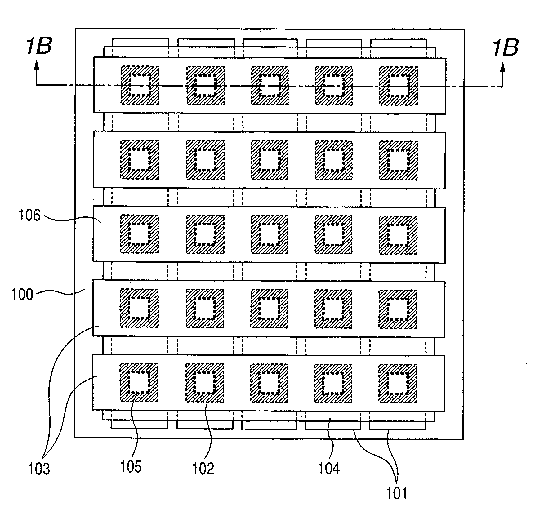
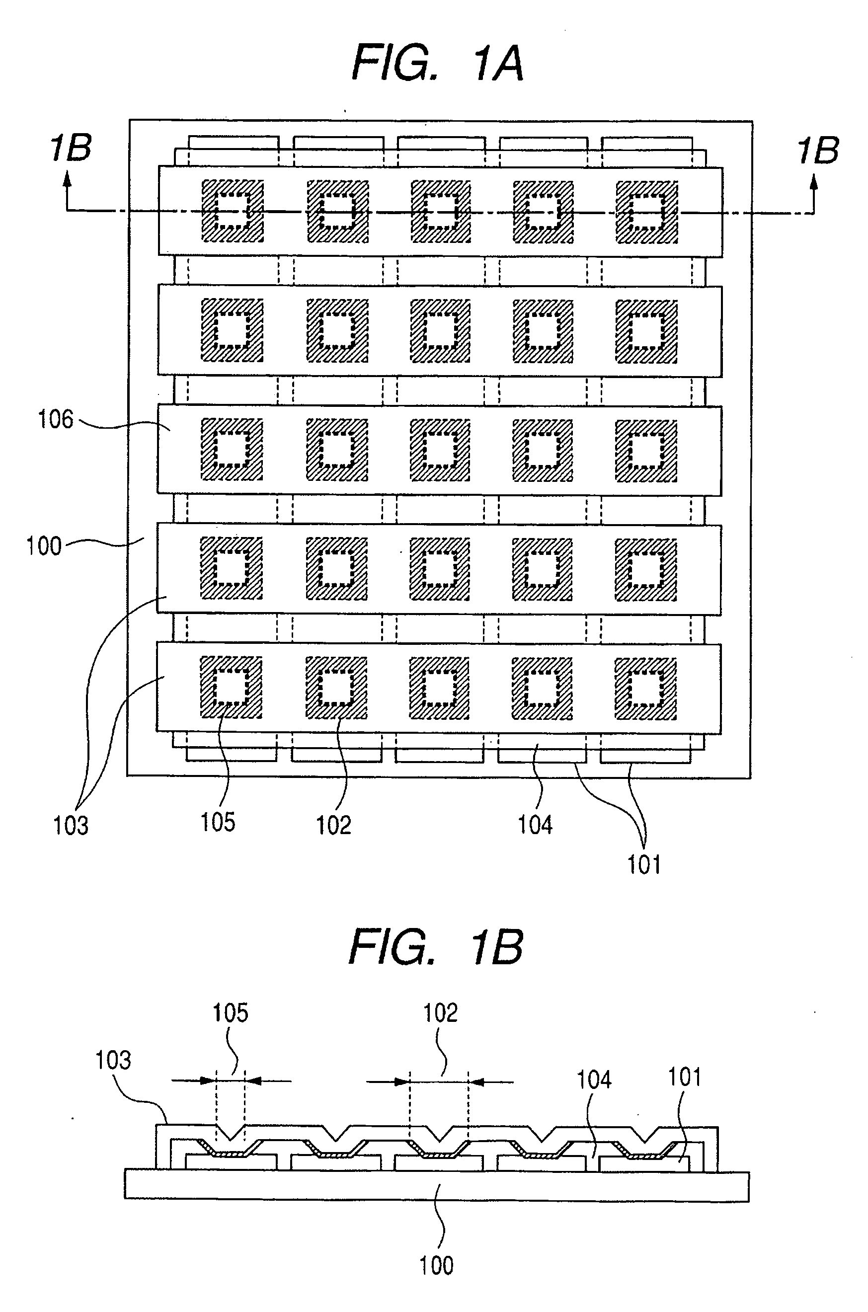
[0095] A simple matrix type organic EL display having the constitution shown in FIGS. 1A and 1B and capable of displaying a full color was prototyped.
[0096] First, an ITO film having a thickness of 400 nm was deposited onto the surface of the no-alkali glass substrate 100 measuring 100 mm long by 100 mm wide by 1.1 mm thick by means of a sputtering method. Then, the resultant was patterned with stripes each having a width of 100 μm at a pitch of 125 μm by means of a photolithography method, whereby the lower electrodes 101 were formed. Upon the formation of the device separation film 104 and the organic compound layers 102 in the subsequent steps, a pattern and a mask were designed in such a manner that these films would not lie on the end portions of the stripes of the lower electrodes 101 after the completion of the steps.
[0097] A solution of a precursor (polyamic acid) for a non-photosensitive polyimide (“PIX-3400”, manufactured by Hitachi Chemical Co., Ltd.) was applied by mea...
example 2
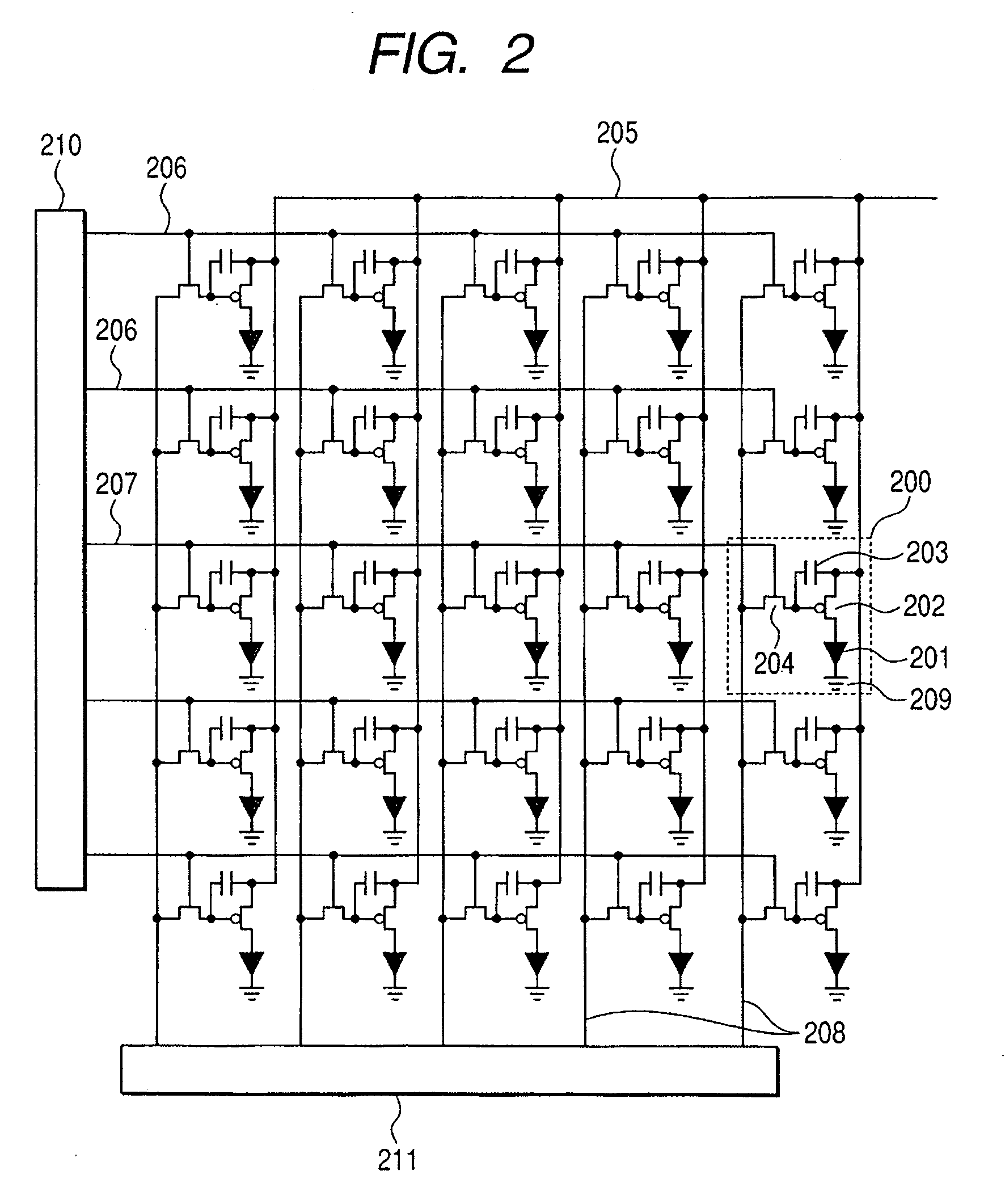
[0104] An active matrix type organic EL display having the sectional constitution shown in FIG. 3 and the circuit constitution shown in FIG. 2 and having a full color display was prototyped.
[0105] First, an undercoat layer composed of silicon oxide (not shown) was formed on the surface of the no-alkali glass substrate 300 measuring 100 mm long by 100 mm wide by 1.1 mm thick. After that, amorphous silicon was deposited onto the resultant by means of a plasma CVD method. Then, the resultant was subjected to laser annealing, following by being polysilicon. Furthermore, a region to be used as the drive transistor 305 (202) or as the switching transistor 204 was formed by means of a photolithography method. In addition, the first metal layer 302 was deposited, and the lower electrode of the capacitor 306, the power source line 205, and the signal line 208 were formed by means of a photolithography method. Furthermore, the silicon oxide film 303 serving as a gate insulating film was depo...
PUM
| Property | Measurement | Unit |
|---|---|---|
| Temperature | aaaaa | aaaaa |
| Fraction | aaaaa | aaaaa |
| Fraction | aaaaa | aaaaa |
Abstract
Description
Claims
Application Information
 - R&D Engineer
- R&D Manager
- IP Professional
- Industry Leading Data Capabilities
- Powerful AI technology
- Patent DNA Extraction
Browse by: Latest US Patents, China's latest patents, Technical Efficacy Thesaurus, Application Domain, Technology Topic.
© 2024 PatSnap. All rights reserved.Legal|Privacy policy|Modern Slavery Act Transparency Statement|Sitemap