Grouping systematic defects with feedback from electrical inspection

Active Publication Date: 2007-03-08
APPLIED MATERIALS INC
View PDF2 Cites 93 Cited by
  • Summary
  • Abstract
  • Description
  • Claims
  • Application Information

AI Technical Summary

Benefits of technology

[0015] One embodiment provides a computer-implemented method for categorizing defects in fabrication of a semiconductor wafer. The method generally includes determining locations of defects on the semiconductor wafer, determining if a set of defect areas, each surrounding a different one of the defects, each contain one or more common structural elements, and if so, categorizing the defects surrounded by the set of defect areas, as corresponding to the common structural elements.
[0016] Another embodiment provides another computer-implemented method for categorizing defects in fabrication of a semiconductor wafer. The method generally includes generating a set of defect clips, each surrounding a different one of the defects and containing one or more structural elements. The method further includes, for each clip, determining if the structural elements in that clip match the structural elements in another clip and, if so categorizing that clip and the other clip as corresponding to the matching structural elements. The method further includes providing an indication of the quantity of defects, for at least some portion of the wafer, categorized as belonging different structural elements.
[0017] Another

Problems solved by technology

In some cases, these repetitive structures may exhibit specific failure modes due to an interaction of the layout with a specific process module used in the manufacturing flow.
In some cases, there may be systematic defects in structures that arise from a variety of causes.
These causes may include imperfections in the deposition, patterning or removal of a specific material or structure.
Defects may also be caused by shifting process parameters, such as deposition, lithographic, etch or other parameters.
Some defects also arise due to design-process interactions (DPI defects).
In other words, DPI defects arise due to the sensitivity of particular designs to process variations, such as variations in deposition, lithographic, etch, or other parameters.
Unfortunately, the sheer volume of these defects makes it challenging to extract meaningful data regarding DPI defects.
The individual defects typically identify locations where a critical dimension (CD) has deviated beyond an acceptable tolerance (possibly le

Method used


Image

  • Grouping systematic defects with feedback from electrical inspection
  • Grouping systematic defects with feedback from electrical inspection
  • Grouping systematic defects with feedback from electrical inspection

Examples


Embodiment Construction

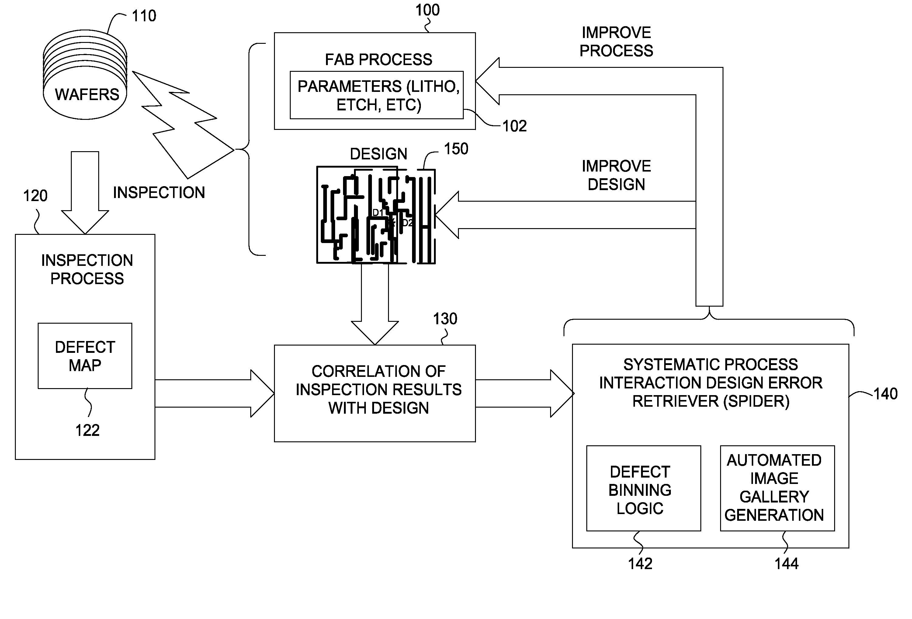
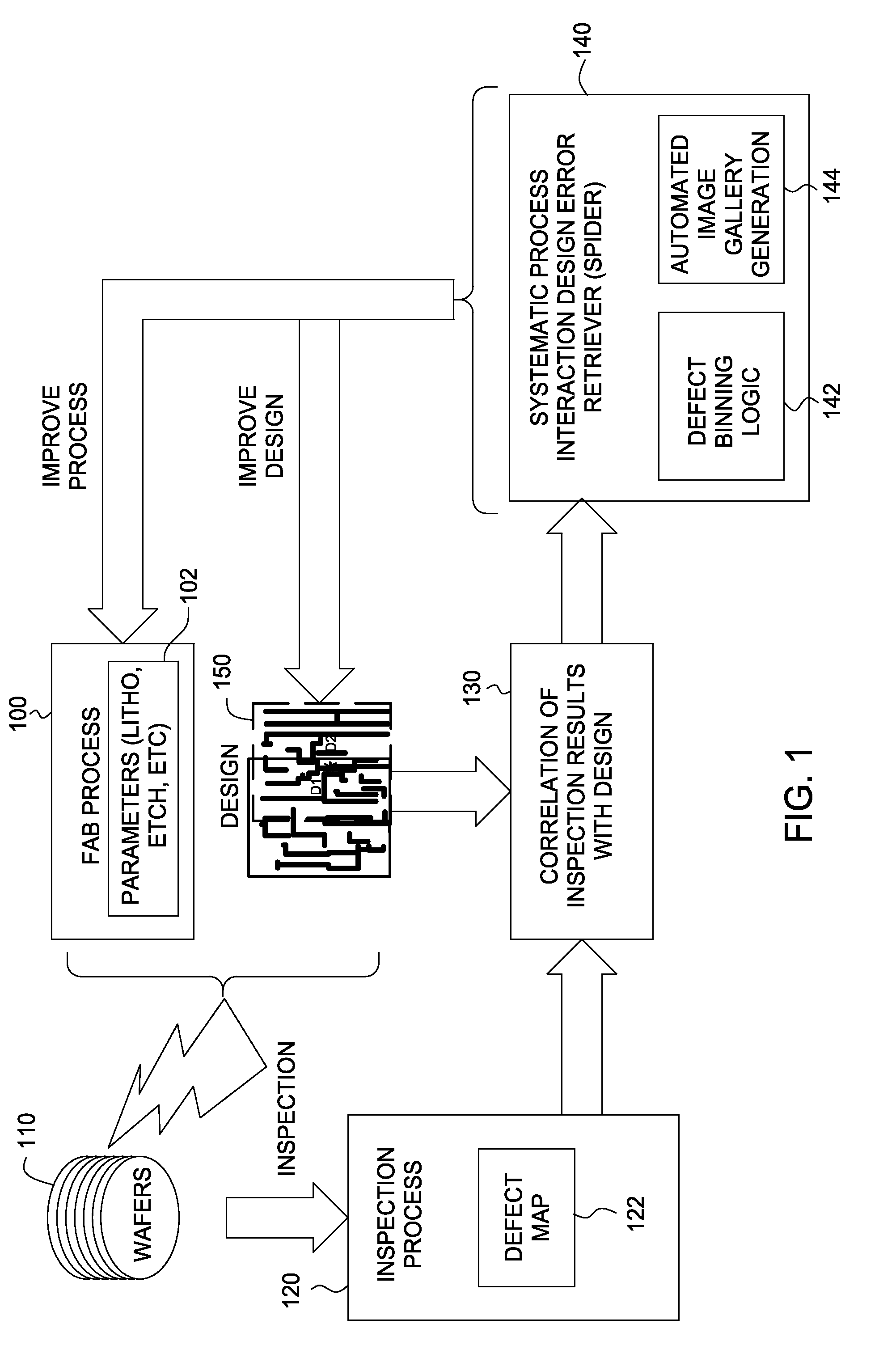
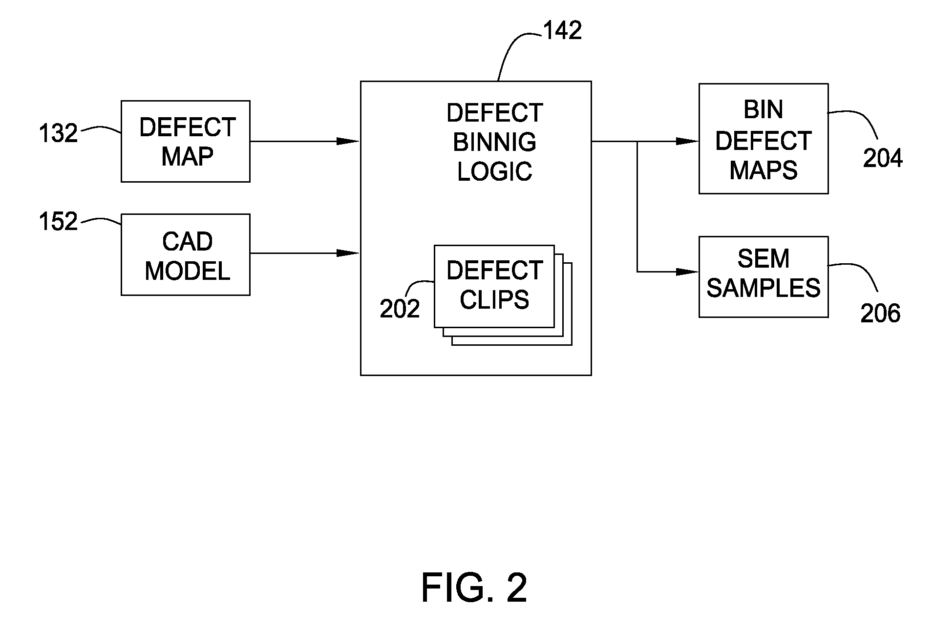
[0040] Embodiments of the present invention generally provide methods and apparatus for detecting defects on workpieces, such as semiconductor wafers and masks used in lithographically writing patterns into such wafers. For some embodiments, by analyzing the layout in the neighborhood of the defect, and matching it to similar defected neighborhoods in different locations across the die, defects may be categorized by common structures in which they occur. This automated categorization allows critical structures to be identified for further investigation into the relationship of design features and / or process parameters (design process interaction) that cause the corresponding defects.

[0041] For some embodiments, software simulations (e.g., OPC modeling or Chemical Mechanical Planarization) may be performed to generate a list of failure-potential locations (hot-spots) across a die. Inspection of actual detected defects may indicate that not all of the predicted failure locations resu...


PUM


Abstract

Methods and apparatus for categorizing defects on workpieces, such as semiconductor wafers and masks used in lithographically writing patterns into such wafers are provided. For some embodiments, by analyzing the layout in the neighborhood of the defect, and matching it to similar defected neighborhoods in different locations across the die, defects may be categorized by common structures in which they occur.

Description

CROSS-REFERENCE TO RELATED APPLICATIONS [0001] The present invention is a continuation-in-part of U.S. patent application Ser. No. 11 / 383,395 filed May 15, 2006, which claims benefit of U.S. provisional application Nos. 60 / 740,408, filed Nov. 28, 2005, 60 / 681,095, filed May 13, 2005, and 60 / 684,360, filed May 24, 2005, all of which are herein incorporated by reference in their entirety.BACKGROUND OF THE INVENTION [0002] 1. Field of the Invention [0003] Embodiments of the present invention generally relate to detecting defects in semiconductor products and, more particularly, to classifying and grouping systematic and random defects. [0004] 2. Description of the Related Art [0005] Semiconductor devices, such as integrated circuits, are typically designed based on repetitive structures such as individual logic cells or larger blocks that perform a specific electrical function. In some cases, these repetitive structures may exhibit specific failure modes due to an interaction of the la...

Claims


Application Information

Patent Timeline
IPC IPC(8): G01N21/84
CPCG03F7/7065G03F1/84
Inventor ORBON, JACOB J.NEHMADI, YOUVALBOKOBZA, OFERBEN-PORATH, ARIELRAVID, EREZSHIMSHI, RINATSVIDENKO, VICKY
Owner APPLIED MATERIALS INC
Why Eureka
Try Eureka