
Wafer having scribe lanes suitable for sawing process, reticle used in manufacturing the same, and method of manufacturing the same

a technology of scribe lanes and sawing process, which is applied in the direction of photomechanical equipment, instruments, originals for photomechanical treatment, etc., can solve the problems of short circuiting of wires in multi-chip packages, chip defects, etc., and achieve the effect of reducing chipping and peeling

Active Publication Date: 2007-03-15
SAMSUNG ELECTRONICS CO LTD
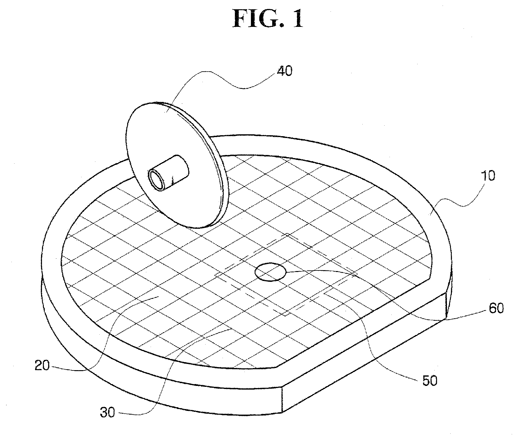
View PDF9 Cites 9 Cited by
  • Summary
  • Abstract
  • Description
  • Claims
  • Application Information

AI Technical Summary

Benefits of technology

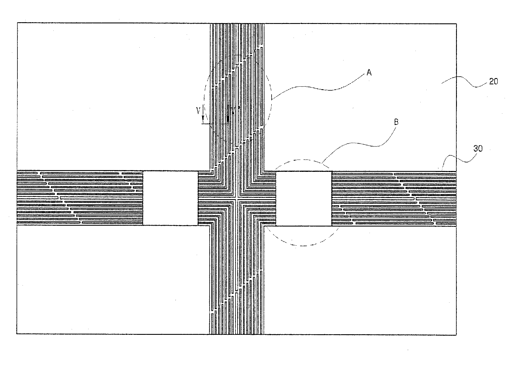
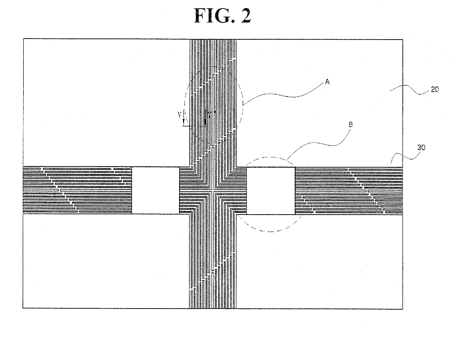
[0011] Providing a plurality of openings such as slits in the scribe lane areas minimizes chipping and peeling during a sawing process as compared to the conventional process.

Problems solved by technology

However, in the conventional sawing process, chipping occurs in each chip due to mechanical stress caused by the blade, and worse, cracks occur in a passivation film and an interlayer insulating film of the chip, thereby causing defects in the chip.
In particular, the undesirable peeling may cause short circuiting of wires in a multi-chip package.

Method used


Image

  • Wafer having scribe lanes suitable for sawing process, reticle used in manufacturing the same, and method of manufacturing the same
  • Wafer having scribe lanes suitable for sawing process, reticle used in manufacturing the same, and method of manufacturing the same
  • Wafer having scribe lanes suitable for sawing process, reticle used in manufacturing the same, and method of manufacturing the same

Examples


Embodiment Construction

[0023] Advantages and features of the invention and methods of accomplishing the same may be understood more readily by reference to the following detailed description of preferred embodiments and the accompanying drawings. The invention may, however, be embodied in many different forms and should not be construed as being limited to the embodiments set forth herein. Rather, these embodiments are provided so that this disclosure will be thorough and complete and will convey the concept of the invention to those skilled in the art. Accordingly, processes, element structures, and technologies known in some embodiments are not specifically described to avoid ambiguity. Like reference numerals refer to like elements throughout the specification.

[0024] Terms used in the present specification are used to describe embodiments, and do not limit the invention. Terms ‘comprise’ and / or ‘comprising’ used in the present specification are used so as not to exclude that described components, proc...


PUM


Abstract

A wafer that is less susceptible to chipping or peeling during a sawing process is disclosed. The wafer includes a plurality of chips, scribe lanes formed between the plurality of chips, and a passivation film, which is formed on the plurality of chips and the scribe lanes and has a plurality of perforations, e.g. slit patterns engraved on each scribe lane. A photolithography reticle and method of manufacturing the wafer are also provided.

Description

CROSS-REFERENCE TO RELATED APPLICATION [0001] This application claims priority from Korean Patent Application No. 10-2005-0085294 filed on Sep. 13, 2005 in the Korean Intellectual Property Office, the contents of which are incorporated herein by reference in their entirety. BACKGROUND [0002] 1. Technical Field [0003] The disclosure relates to a wafer having scribe lanes suitable for a sawing process, a reticle used in manufacturing the wafer, and a method of manufacturing the wafer. [0004] 2. Description of the Related Art [0005] Generally, after a plurality of chips are formed on a wafer, a sawing process is performed. In the sawing process, a diamond blade rotating at high speed cuts the wafer along scribe lanes to separate the chips from one another. [0006] However, in the conventional sawing process, chipping occurs in each chip due to mechanical stress caused by the blade, and worse, cracks occur in a passivation film and an interlayer insulating film of the chip, thereby causi...

Claims


Application Information

Patent Timeline
Patent Type & Authority Applications(United States)
IPC IPC(8): H01L23/544
CPCG03F1/14H01L21/78H01L23/5256H01L23/544H01L23/562H01L2924/0002H01L2223/54453H01L2924/00G03F1/44
Inventor YANG, HUNG-MO
Owner SAMSUNG ELECTRONICS CO LTD
Learn More