Plasma display device and method for driving the same

Inactive Publication Date: 2007-04-26
LG ELECTRONICS INC
View PDF4 Cites 0 Cited by
  • Summary
  • Abstract
  • Description
  • Claims
  • Application Information

AI Technical Summary

Benefits of technology

[0014] An object of the present invention is to provide a plasma display device and a method for driving the same capable of preventing faulty discharge occurring during in

Problems solved by technology

Accordingly, when a driving voltage is applied between the X-electrode and the Y-electrode during driving of a display, opposed discharge occurs between the X-electrode and the Y-electrode, causing wall charge.
However, the related art plasma display device is problematic in that erroneous discharge occurs since power is simultaneously supplied to the X, Y and Z boards 120, 130 and 140 during initial driving of the pla

Method used


Image

  • Plasma display device and method for driving the same
  • Plasma display device and method for driving the same
  • Plasma display device and method for driving the same

Examples


Embodiment Construction

[0025] Reference will now be made in detail to the preferred embodiments of the present invention, examples of which are illustrated in the accompanying drawings. Wherever possible, the same reference numbers will be used throughout the drawings to refer to the same or like parts.

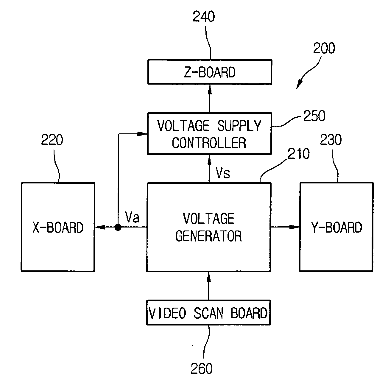
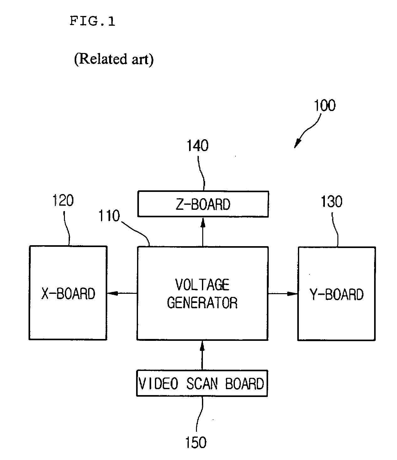
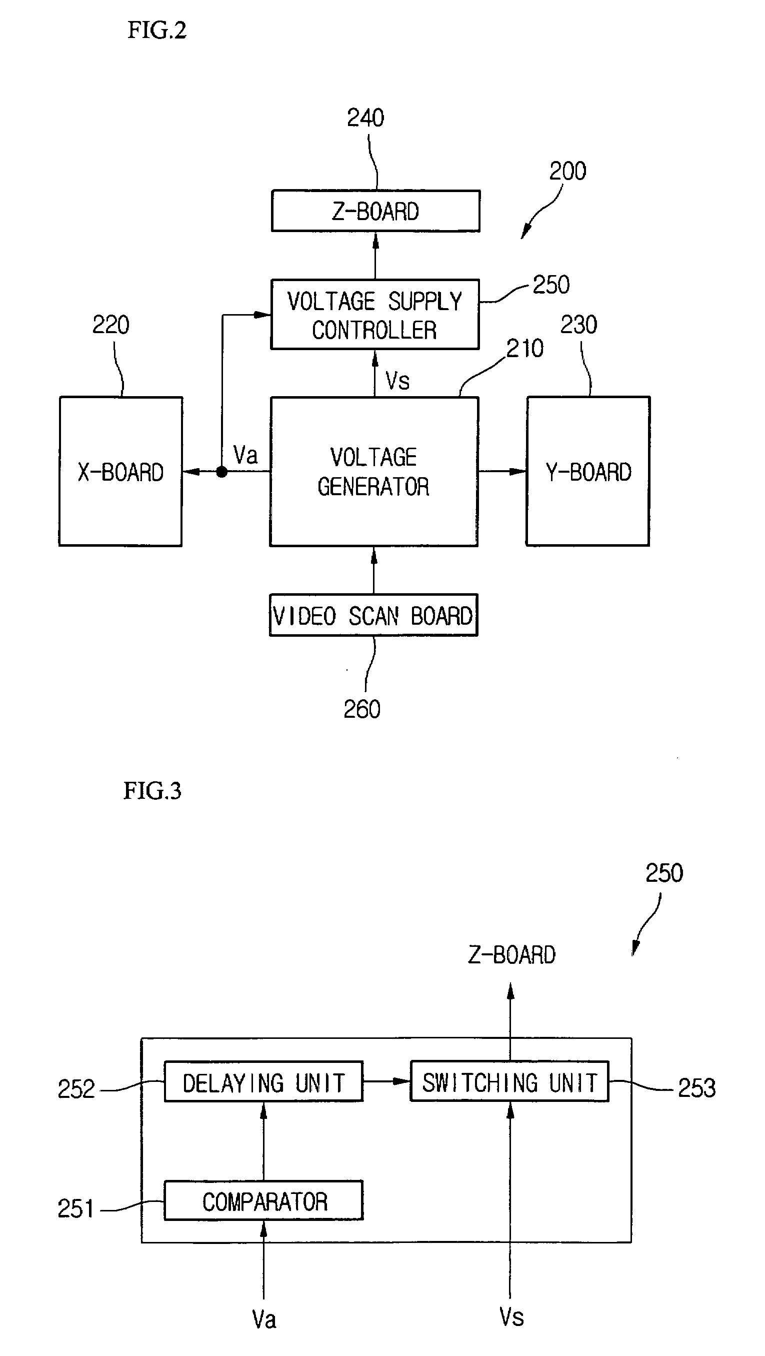
[0026]FIG. 2 is a block diagram illustrating a structure of a plasma display device according to an embodiment of the present invention. Although a power supply controller is installed only toward a Z-board in FIG. 2, the present invention is not limited thereto, but it is obvious that the power supply controller may be installed toward another board if necessary.

[0027] First, as illustrated in FIG. 2, a plasma display device 200 according to an embodiment of the present invention may include a voltage generator 210, an X-board 220, a Y-board 230, a Z-board 240, a power supply controller 250, and a video scan board 260 to provide power individually to an address electrode, a scan electrode, and a sustain ...


PUM


Abstract

A plasma display device is provided. The plasma display device includes an X-board, a Y-board, a Z-board, a voltage generator, and a power supply controller. The X-board outputs an address voltage to an address electrode. The Y-board outputs a scan voltage to a scan electrode. A Z-board outputs a sustain voltage to a sustain electrode. A voltage generator generates the address voltage, the scan voltage and the sustain voltage, and provides the address voltage, the scan voltage and the sustain voltage to the X-board, the Y-board and the Z-board, respectively. The power supply controller controls transmission of the address voltage, the scan voltage, and the sustain voltage to provide power to at least one of the X-board, the Y-board and the Z-board at a different time when the display device is initially driven.

Description

BACKGROUND OF THE INVENTION [0001] 1. Field of the Invention [0002] The present invention relates to a plasma display device, and more particularly, to a plasma display device and a method for driving the same. [0003] 2. Description of the Related Art [0004] In general, a plasma display device includes a scan electrode (hereinafter, referred to as a ‘Y electrode’) and a sustain electrode (hereinafter, referred to as a ‘Z-electrode’) on the same plane of an upper substrate, and an address electrode (hereinafter, referred to as an. ‘X electrode’) on a lower substrate. Also, a barrier rib is formed between the X-electrodes to prevent cross-talk, and a phosphor layer is formed around the barrier rib and the X-electrode. Also, a space between the upper substrate and the lower substrate is filled with an inert gas, thereby forming a discharge region. [0005] Accordingly, when a driving voltage is applied between the X-electrode and the Y-electrode during driving of a display, opposed disch...

Claims


Application Information

Patent Timeline
IPC IPC(8): G09G3/28
CPCG09G3/28G09G2330/02G09G2330/026G09G3/296
Inventor PARK, JUNG HYUN
Owner LG ELECTRONICS INC
Why Eureka
Try Eureka