Supercharge Your Innovation With Domain-Expert AI Agents!

Display device and method of repairing the same

a technology of a display device applied in the field of display devices and a repair method, can solve the problems of increased short-circuit defects, luminescent spot defects, and defects, and achieve the effect of positive repair of defective products

Inactive Publication Date: 2007-05-31
MITSUBISHI ELECTRIC CORP
View PDF6 Cites 0 Cited by
  • Summary
  • Abstract
  • Description
  • Claims
  • Application Information

AI Technical Summary

Benefits of technology

[0013] According to the present invention, it is possible to positively repair a defective product caused by a pixel defect such as a luminescent spot defect in a semi-transmission type display device.

Problems solved by technology

When the panel interval is reduced and when foreign objects generated in the manufacturing process are attached to a portion between the panels before the process in which the array board and the color filter board are bonded to each other, defects of short-circuit are increased because of the existence of the foreign objects between the panels.
In the case where a short-circuit is caused and a pixel electrode on the array board and an opposing electrode on the color filter board are electrically continued to each other, defects of luminescent spots are caused on the display having a structure of the normally white mode.
Accordingly, for the above structural reason, the semi-transmission type display device is disadvantageous in that defects of luminescent spots, which are caused by the existence of foreign objects, are increased.
Especially, when defects of luminescent spots are generated in the display device, it will be immediately rejected as a defective product.
Therefore, it is expected that the repaired portion becomes a black spot.
As compared with the luminescent spot in the reflecting display state, the luminescent spot in the transmitting display state is a serious defect.
As a result, the following problem is encountered.
It is impossible to change the repaired pixel into a perfect black spot, that is, the repaired pixel can be only changed into a defective spot having some luminance.
However, the following problems may be encountered in the irradiation of the laser beam.
When the counter electrode is damaged on the color filter board, by an influence of the scattered scraps (foreign objects), the array board and the color filter board are short-circuited to each other, and a defect is generated again.
When a black matrix portion, which is a shading region of the color filter board, is damaged, light leaks out from the thus damaged shading region at the time of lighting, which can be a cause of a defective product.

Method used


Image

  • Display device and method of repairing the same
  • Display device and method of repairing the same
  • Display device and method of repairing the same

Examples


first embodiment

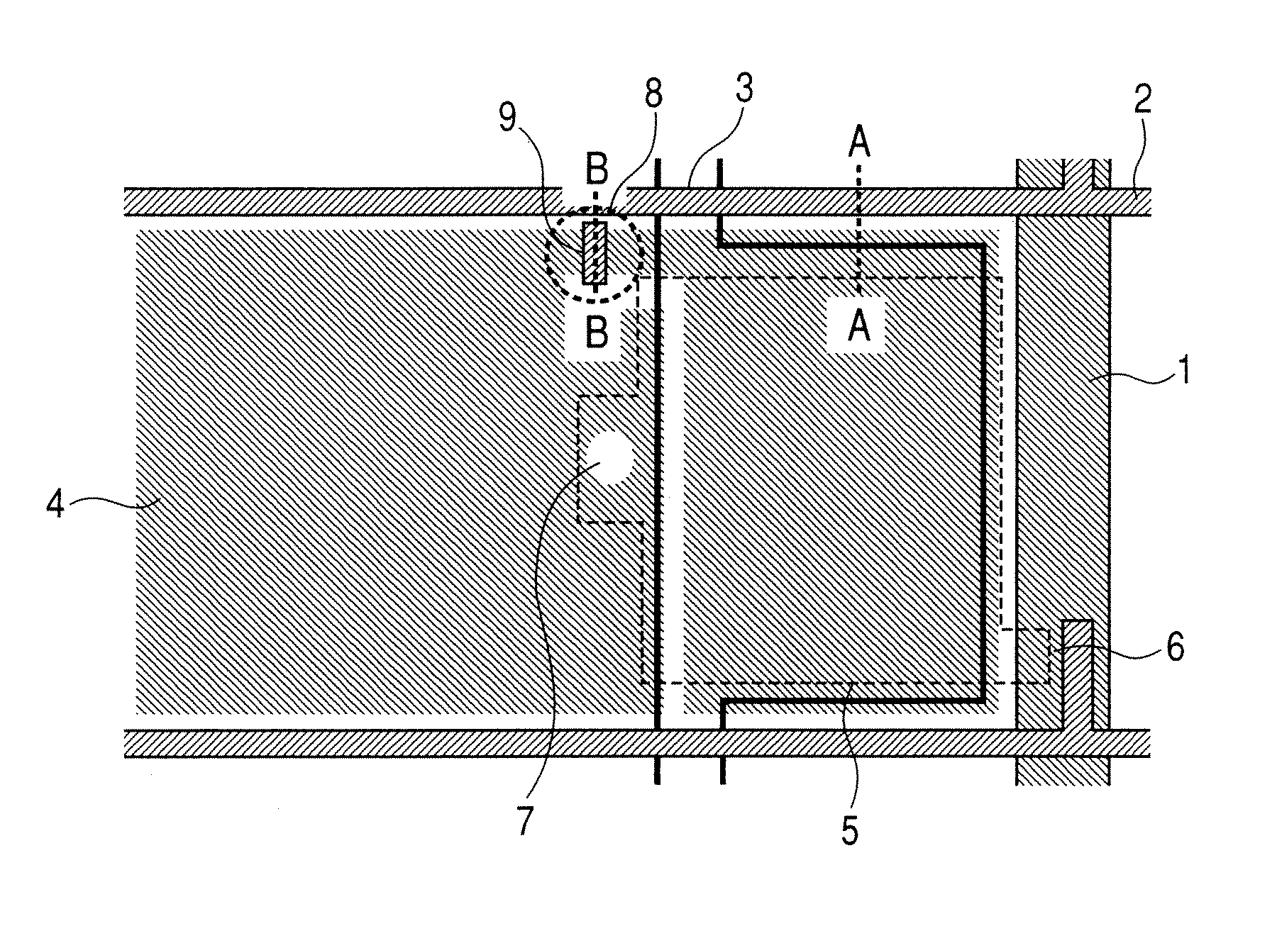
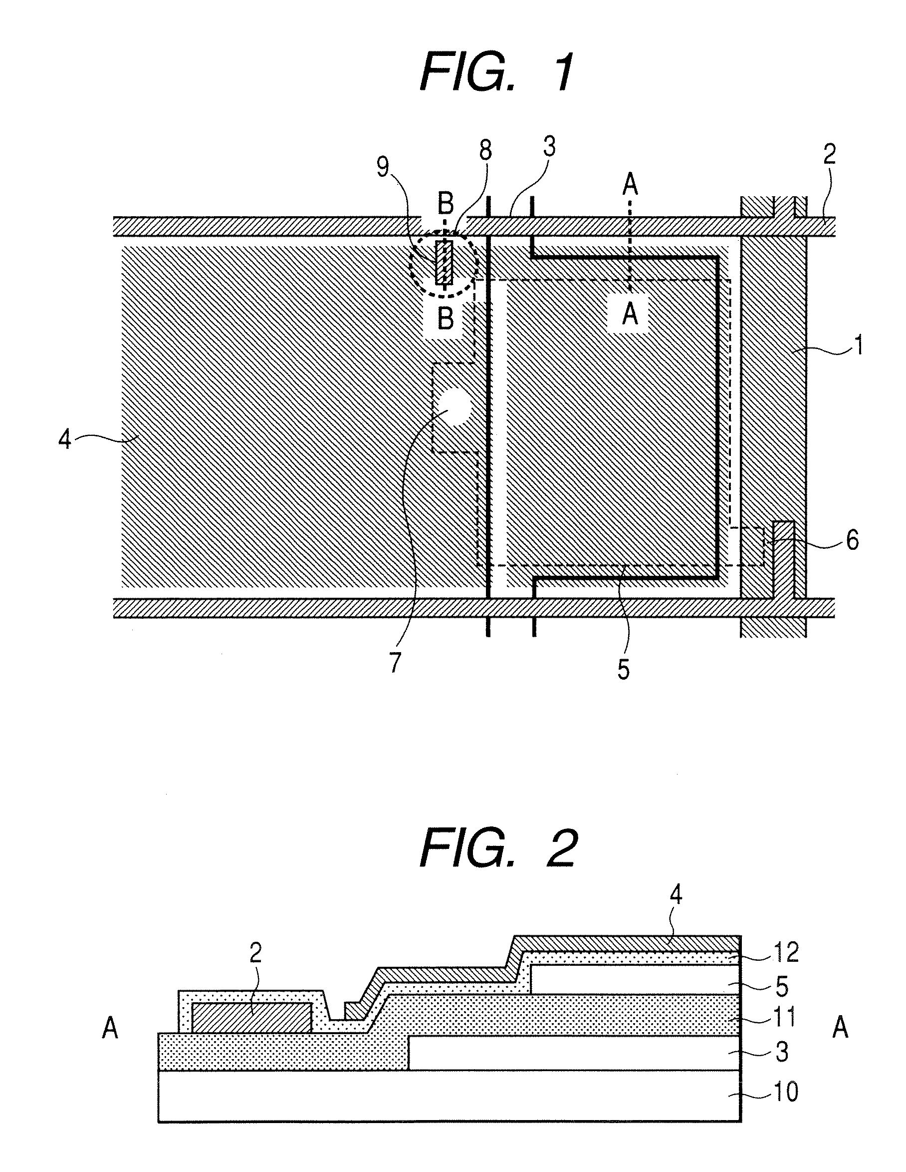
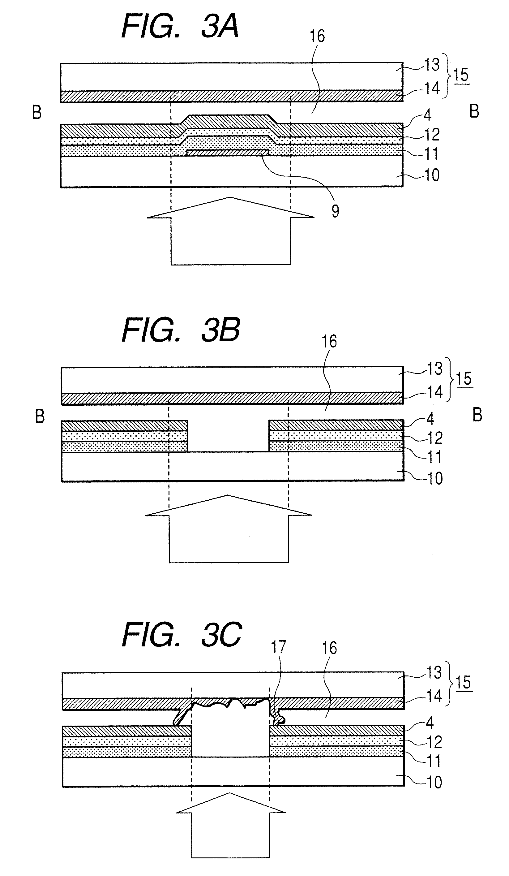
[0019] Referring to FIGS. 1 to 3, the First Embodiment of the present invention will be explained below. FIG. 1 is a plan view of a substantial one pixel in Embodiment 1 of the present invention, FIG. 2 is a sectional view taken on line A-A in FIG. 1, and FIGS. 3A to 3C are sectional views taken on line B-B in FIG. 1.

[0020] In FIG. 1, a common wiring 3 is formed in parallel with a scanning line (gate wiring) 1 formed on an insulating board (array board) 10. A video signal line (source line) 2 is formed in a direction perpendicular to the scanning line 1 and the common line 3 while an insulating film 11 is being interposed between the video signal line 2 and the scanning line 1 and common lines 3. A substantial left half region of FIG. 1 corresponds to the transmitting region in the semi-transmission type display device. In the transmitting region, a pixel electrode 4 including a transparent conductive film such as ITO is formed. In the reflecting region, which is a substantial righ...

second embodiment

[0027] Referring to FIG. 4, the Second Embodiment of the present invention will be explained below. FIG. 4 is a plan view of substantial one pixel in the Second Embodiment of the present invention. In FIG. 4, like reference characters are used to indicate like parts in FIGS. 1 to 3.

[0028] Referring to FIG. 4, different points of Embodiment 2 from Embodiment 1 will be explained below. According to the structure shown in FIG. 4, the transparent conductive film is not substantially formed on the reflecting electrode 5 in the reflecting region to which foreign objects between the panels tend to attach. The reflecting electrode 5 is not exposed. When voltage is impressed upon the liquid crystal layer via the protective film 12 formed on the upper layer, even if no transparent conductive film is formed in the reflecting region, a display of reflection is not affected. In this connection, the structure of this embodiment can be applied to the following case. The effective voltage to be im...


PUM

PropertyMeasurementUnit
widthaaaaaaaaaa
transparent conductiveaaaaaaaaaa
widthaaaaaaaaaa

Abstract

A display device has a pixel including a transmitting region to transmit light and a reflecting region to reflect external light. The display device includes: a transparent conductive film containing a first transparent conductive film forming a pixel electrode in the transmitting region, a second transparent conductive film provided as an upper layer of a reflecting electrode forming the reflecting region, and a connecting portion integrally formed with and connecting the first transparent conductive film and the second transparent conductive film; and a opaque conductive film provided as a lower layer of the transparent conductive film, and located below an area of the transparent conductive film including the connection portion.

Description

BACKGROUND OF THE INVENTION [0001] 1. Field of the Invention [0002] The present invention relates to a display device and a method of repairing the same. More particularly, the present invention relates to a display device and a method of repairing the same which is preferably applied to a method of repairing a defective pixel in a semi-transmission type display device. [0003] 2. Background Art [0004] Recently, flat panel displays (FPD) such as liquid crystal displays have been widely applied to monitors for personal computer use, monitors for television use and monitors for portable terminal use. Especially, in the field of mobile phones, portable type terminal devices have made a rapid progress. It is important that the portable type terminal devices are compact and capable of driving over a long period of time. In view of the above circumstances, a semi-transmission type display device is watched with keen interest, which is capable of saving electric power consumption in such a ...

Claims


Application Information

Patent Timeline
Patent Type & Authority Applications(United States)
IPC IPC(8): G02F1/1335G02F1/1333
CPCG02F1/1309G02F1/133555G02F1/1335G02F1/1343
Inventor MURAKAMI, KATSUAKI
Owner MITSUBISHI ELECTRIC CORP
Features
  • R&D
  • Intellectual Property
  • Life Sciences
  • Materials
  • Tech Scout
  • Unparalleled Data Quality
  • Higher Quality Content
  • 60% Fewer Hallucinations
Learn More