Display device and method of repairing the same including transmitting and reflecting regions and an opaque conductive film below a connecting portion
a technology of conductive film and display device, which is applied in the direction of instruments, non-linear optics, optics, etc., can solve the problems of increased short-circuit damage, luminescent spot damage, and defects, and achieve the effect of positive repair of defective products
- Summary
- Abstract
- Description
- Claims
- Application Information
AI Technical Summary
Benefits of technology
Problems solved by technology
Method used
Image

Examples
first embodiment
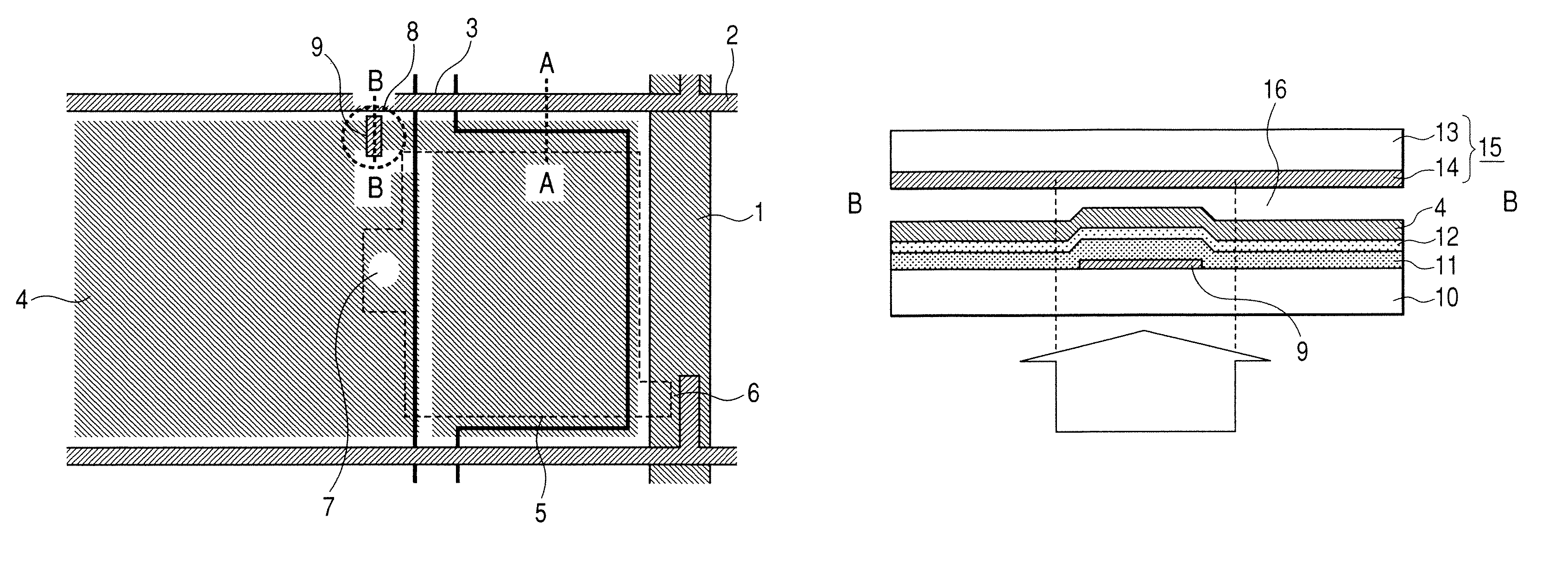
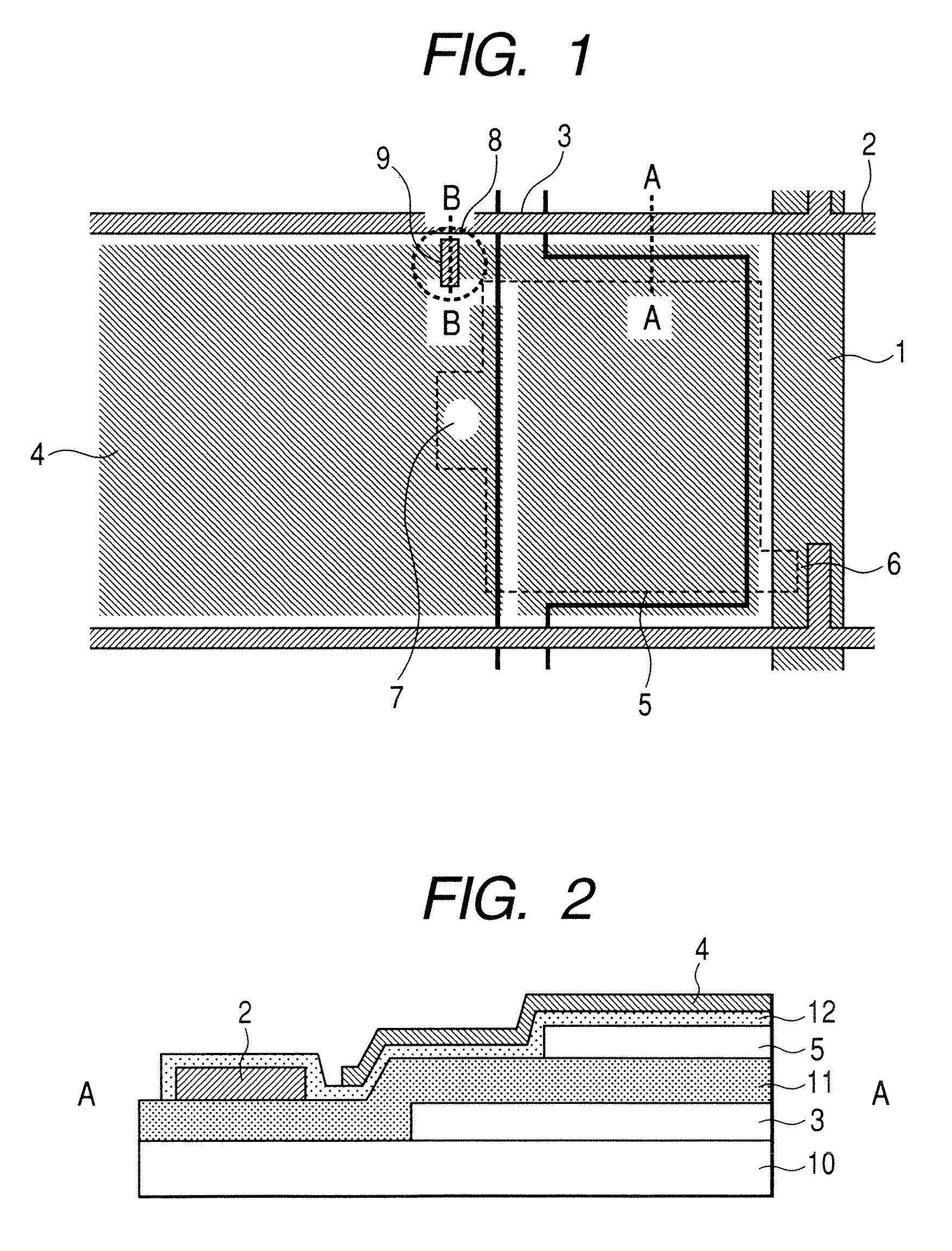
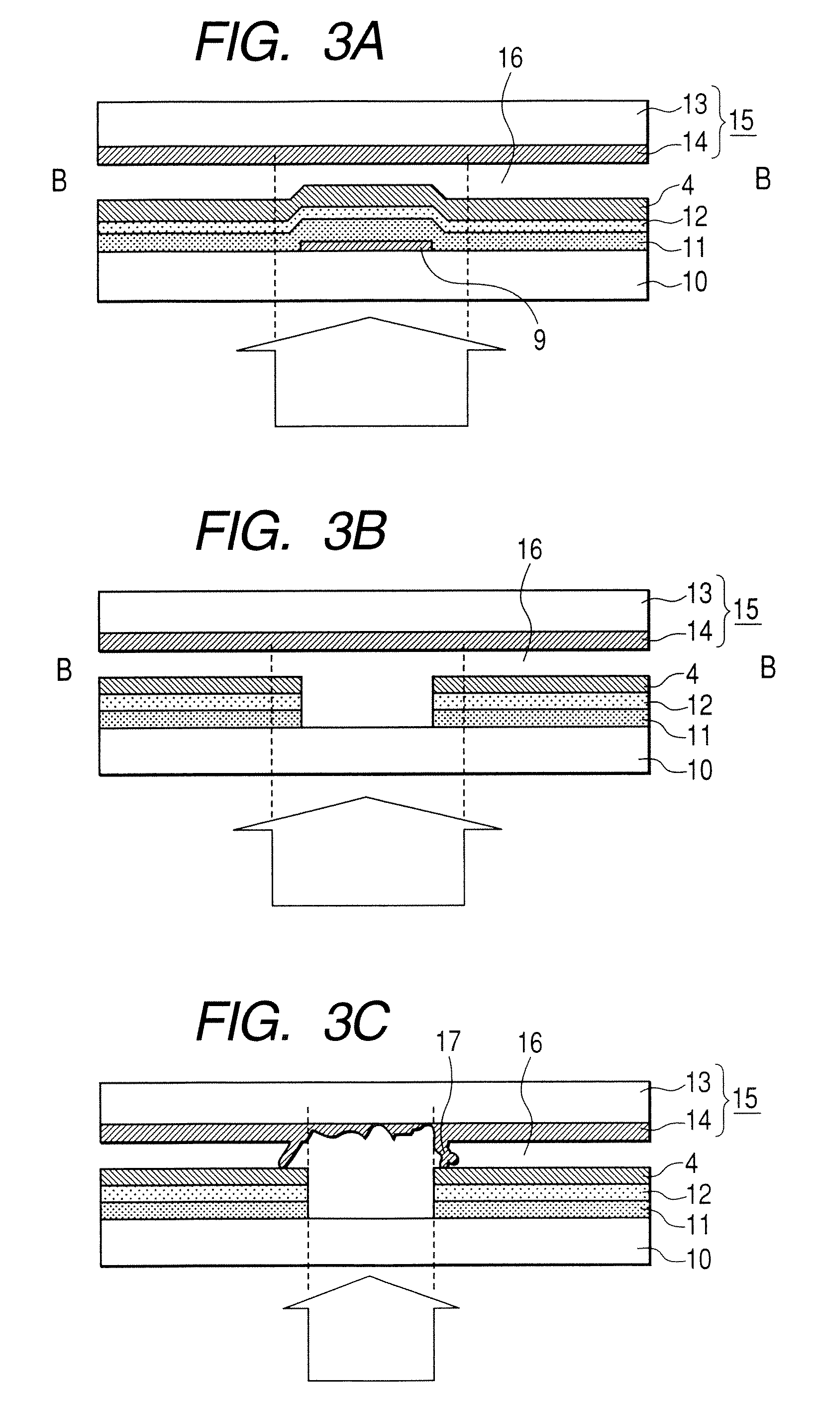
[0019]Referring to FIGS. 1 to 3, the First Embodiment of the present invention will be explained below. FIG. 1 is a plan view of a substantial one pixel in Embodiment 1 of the present invention, FIG. 2 is a sectional view taken on line A-A in FIG. 1, and FIGS. 3A to 3C are sectional views taken on line B-B in FIG. 1.
[0020]In FIG. 1, a common wiring 3 is formed in parallel with a scanning line (gate wiring) 1 formed on an insulating board (array board) 10. A video signal line (source line) 2 is formed in a direction perpendicular to the scanning line 1 and the common line 3 while an insulating film 11 is being interposed between the video signal line 2 and the scanning line 1 and common lines 3. A substantial left half region of FIG. 1 corresponds to the transmitting region in the semi-transmission type display device. In the transmitting region, a pixel electrode 4 including a transparent conductive film such as ITO is formed. In the reflecting region, which is a substantial right h...
second embodiment
[0027]Referring to FIG. 4, the Second Embodiment of the present invention will be explained below. FIG. 4 is a plan view of substantial one pixel in the Second Embodiment of the present invention. In FIG. 4, like reference characters are used to indicate like parts in FIGS. 1 to 3.
[0028]Referring to FIG. 4, different points of Embodiment 2 from Embodiment 1 will be explained below. According to the structure shown in FIG. 4, the transparent conductive film is not substantially formed on the reflecting electrode 5 in the reflecting region to which foreign objects between the panels tend to attach. The reflecting electrode 5 is not exposed. When voltage is impressed upon the liquid crystal layer via the protective film 12 formed on the upper layer, even if no transparent conductive film is formed in the reflecting region, a display of reflection is not affected. In this connection, the structure of this embodiment can be applied to the following case. The effective voltage to be impre...
PUM
| Property | Measurement | Unit |
|---|---|---|
| width | aaaaa | aaaaa |
| transparent conductive | aaaaa | aaaaa |
| transparent | aaaaa | aaaaa |
Abstract
Description
Claims
Application Information
 - R&D
- Intellectual Property
- Life Sciences
- Materials
- Tech Scout
- Unparalleled Data Quality
- Higher Quality Content
- 60% Fewer Hallucinations
Browse by: Latest US Patents, China's latest patents, Technical Efficacy Thesaurus, Application Domain, Technology Topic, Popular Technical Reports.
© 2025 PatSnap. All rights reserved.Legal|Privacy policy|Modern Slavery Act Transparency Statement|Sitemap|About US| Contact US: help@patsnap.com