

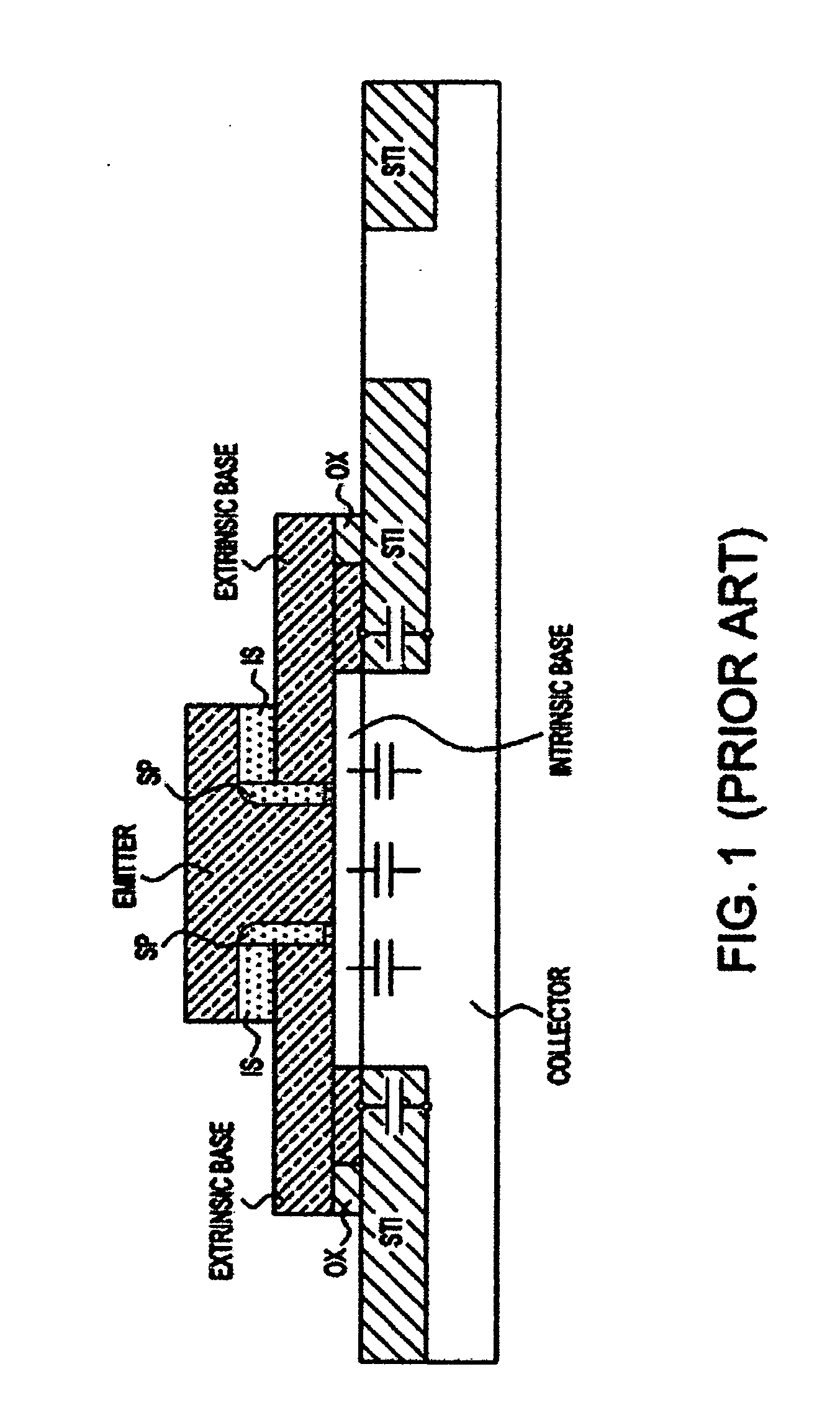
Bipolar junction transistors (BJTS) with second shallow trench isolation (STI) regions, and methods for forming same
a bipolar junction transistor and shallow trench isolation technology, applied in the direction of electrical equipment, semiconductor devices, radio frequency control devices, etc., can solve the problems of limited lithographic process typically used for fabricating active/extrinsic bases, difficult to minimize the overlap of base-collectors, and corresponding increase in base resistan
- Summary
- Abstract
- Description
- Claims
- Application Information
AI Technical Summary
Benefits of technology
Problems solved by technology
Method used
Image

Examples
Embodiment Construction
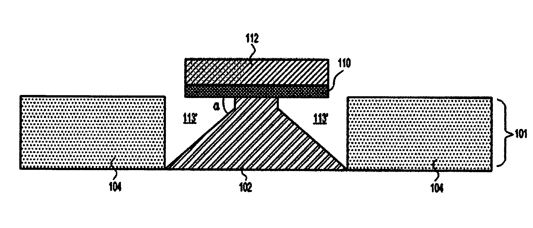
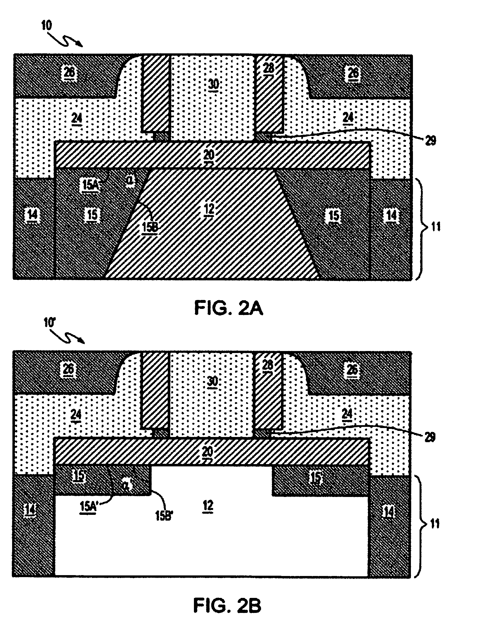
[0025] In the following description, numerous specific details are set forth, such as particular structures, components, materials, dimensions, processing steps and techniques, in order to provide a thorough understanding of the present invention. However, it will be appreciated by one of ordinary skill in the art that the invention may be practiced without these specific details. In other instances, well-known structures or processing steps have not been described in detail in order to avoid obscuring the invention.
[0026] It will be understood that when an element as a layer, region or substrate is referred to as being “on” or “over” another element, it can be directly on or over the other element or intervening elements may also be present. In contrast, when an element is referred to as being “directly on” or “directly over” another element, there are no intervening elements present. It will also be understood that when an element is referred to as being “connected” or “coupled” ...
PUM
 Abstract
Description
Claims
Application Information