Display device and a method of driving the same

a technology of a display device and a drive mechanism, which is applied in the direction of semiconductor devices, instruments, electrical apparatus, etc., can solve the problems of causing the afterimage to appear on the screen, causing the subsequent data voltage to be transformed, and causing the undesirable electric field in the liquid crystal layer to be produced

Active Publication Date: 2007-06-14
SAMSUNG DISPLAY CO LTD
View PDF3 Cites 36 Cited by
  • Summary
  • Abstract
  • Description
  • Claims
  • Application Information

AI Technical Summary

Benefits of technology

[0013] According to still another exemplary embodiment of the present invention, there is provided a display device including a first plate including a gate line connected to a control terminal of a thin film transistor in each pixel, a data line connected to an input terminal of the thin film transistor, a pixel electrode connected to an output terminal of the thin film transistor, and a first impurity adsorption electrode which is electrically isolated from and overlaps with the gate line or the data line and is separated from the pixel electrode, a second plate facing the first plate and including a lattice-shaped black matrix pattern and a second impurity adsorption electrode which is disposed below and overlapped with the black matrix pattern and faces the first impurity adsorption electrode, and a liquid crystal layer interposed between the first plate and the second plate.

Problems solved by technology

The residual DC bias may transform a subsequent data voltage or produce an undesirable electric field in the liquid crystal layer even when no data voltage is supplied.
However, even though inversion driving is performed, a DC bias still remains in a liquid crystal layer due to a change in a kickback voltage, etc.
The distortion may cause an afterimage to appear on a screen.

Method used


Image

  • Display device and a method of driving the same
  • Display device and a method of driving the same
  • Display device and a method of driving the same

Examples


Embodiment Construction

[0030] A display device according to exemplary embodiments of the present invention will now be described with reference to the accompanying drawings. In the following description, the invention will be described with regard to a liquid crystal display; however, the present invention is not limited thereto.

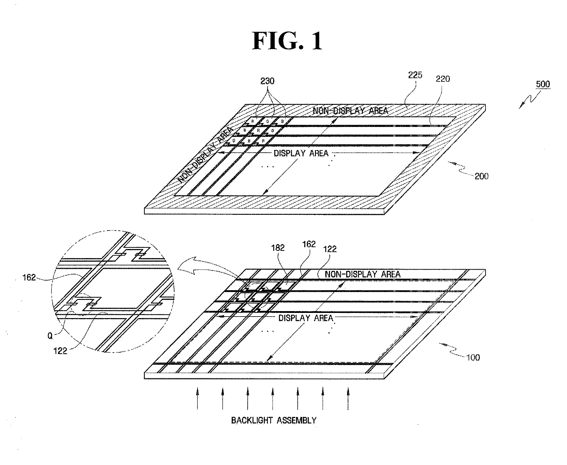
[0031]FIG. 1 is a perspective view of a liquid crystal display 500 according to an exemplary embodiment of the present invention.

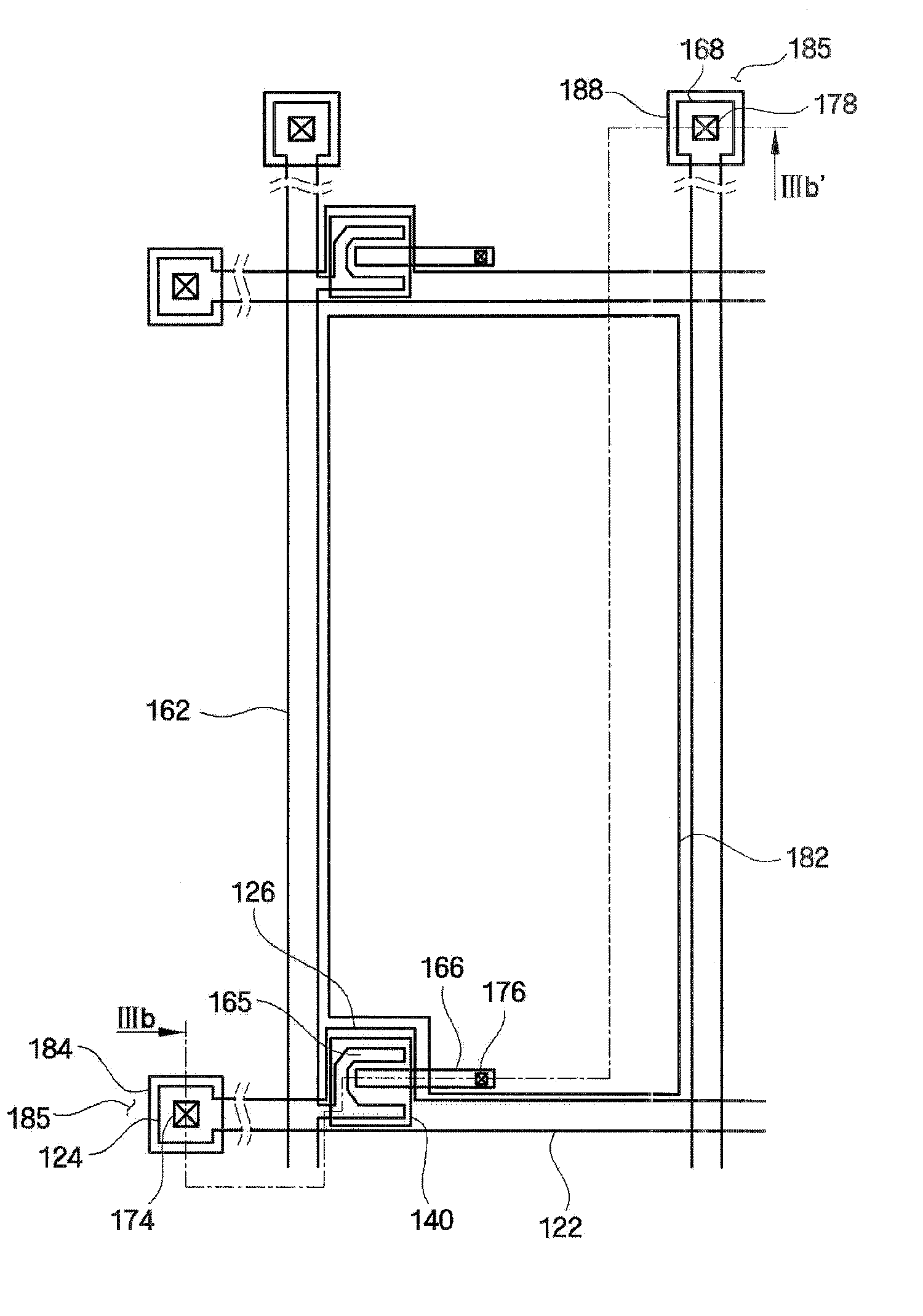
[0032] Referring to FIG. 1, the liquid crystal display 500 includes a first plate 100, a second plate 200 facing the first plate 100, and an intermediate layer (not shown) interposed between the first plate 100 and the second plate 200. Here, the intermediate layer of the liquid crystal display 500 may be a liquid crystal layer including liquid crystal molecules. As used herein, “a panel composed of a first plate, a second plate, and a liquid crystal layer” will also be referred to as a “a liquid crystal panel”.

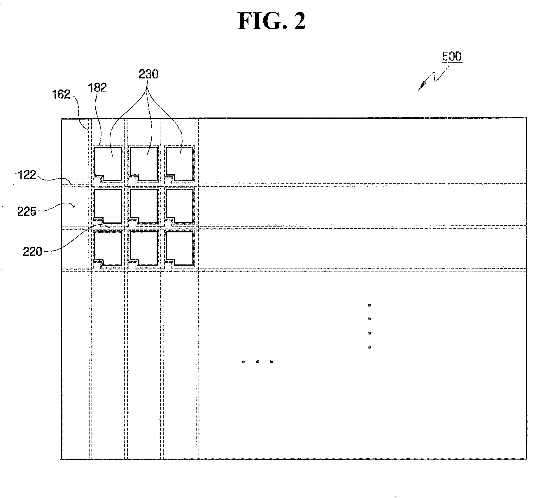
[0033] The first plate 100 includes a pl...


PUM


Abstract

A display device which can suppress an afterimage phenomenon from occurring includes a first plate including a pixel electrode which is disposed in a transmitting region and a first impurity adsorption electrode which is disposed in a light-shielding region and is separated from the pixel electrode, a second plate facing the first plate and including a second impurity adsorption electrode which is disposed in the light-shielding region to face the first impurity adsorption electrode, and an intermediate layer interposed between the first plate and the second plate.

Description

CROSS-REFERENCE TO RELATED APPLICATION [0001] This application claims priority to Korean Patent Application No. 10-2005-0118173, filed on Dec. 6, 2005 in the Korean Intellectual Property Office, the disclosure of which is incorporated by reference herein in its entirety. BACKGROUND OF THE INVENTION [0002] 1. Technical Field [0003] The present invention relates to a display device, and more particularly, to a display device which can suppress an occurrence of an afterimage phenomenon. [0004] 2. Discussion of the Related Art [0005] A liquid crystal display is one of the most widely used flat panel displays. For example, the liquid crystal display is commonly found in a variety of electronic devices such as flat screen televisions, laptop computers, cell phones, and digital cameras. [0006] The liquid crystal display includes two substrates provided with field-generating electrodes such as pixel electrodes and a common electrode and a liquid crystal layer interposed therebetween. The li...

Claims


Application Information

Patent Timeline
Patent Type & Authority Applications(United States)
IPC IPC(8): H01L21/00H01L31/113H01L21/20
CPCG02F1/1333G02F1/133502G02F2001/133388G02F2001/133397G02F1/133388G02F1/133397G02F1/1335
Inventor LEE, JUN-WOOKIM, HEE-SEOPLEE, CHANG-HUNHAN, EUN-HEE
Owner SAMSUNG DISPLAY CO LTD
Why Eureka
Try Eureka