
Display substrate, method of manufacturing the same and display panel having the same

a technology of display substrate and substrate, which is applied in the field of display substrate, can solve the problems of reducing the transmittance affecting the performance of the gate insulating layer, and affecting the performance of the pixel electrod

Active Publication Date: 2007-07-12
SAMSUNG DISPLAY CO LTD
View PDF7 Cites 70 Cited by
  • Summary
  • Abstract
  • Description
  • Claims
  • Application Information

AI Technical Summary

Problems solved by technology

However, the surface of the gate insulating layer may become damaged during the formation of a pixel electrode thereon.
Such surface damage can cause defects in the organic semiconductor formed on the gate insulating layer, resulting in reduced transmittance of the pixel electrode.

Method used


Image

  • Display substrate, method of manufacturing the same and display panel having the same
  • Display substrate, method of manufacturing the same and display panel having the same
  • Display substrate, method of manufacturing the same and display panel having the same

Examples


Embodiment Construction

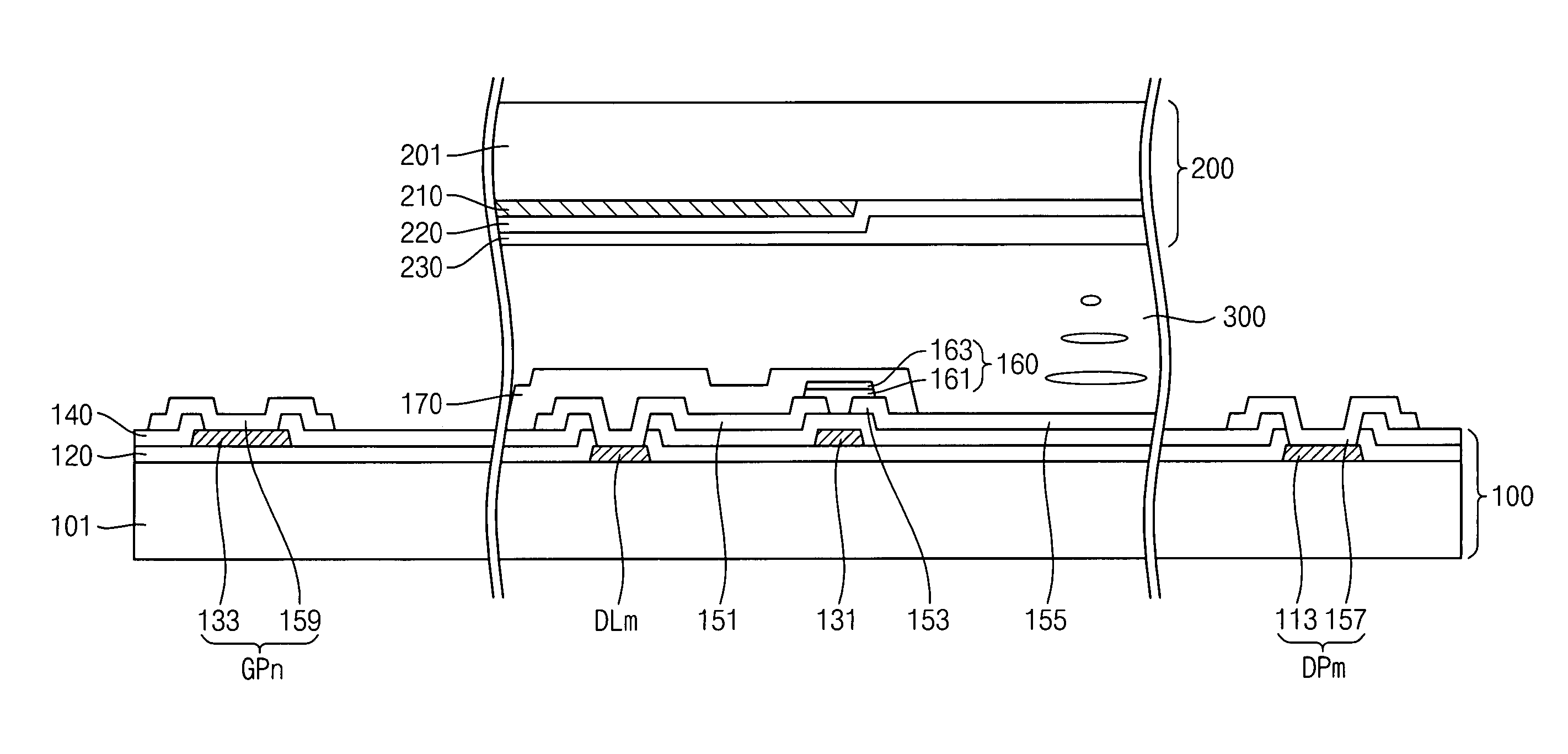
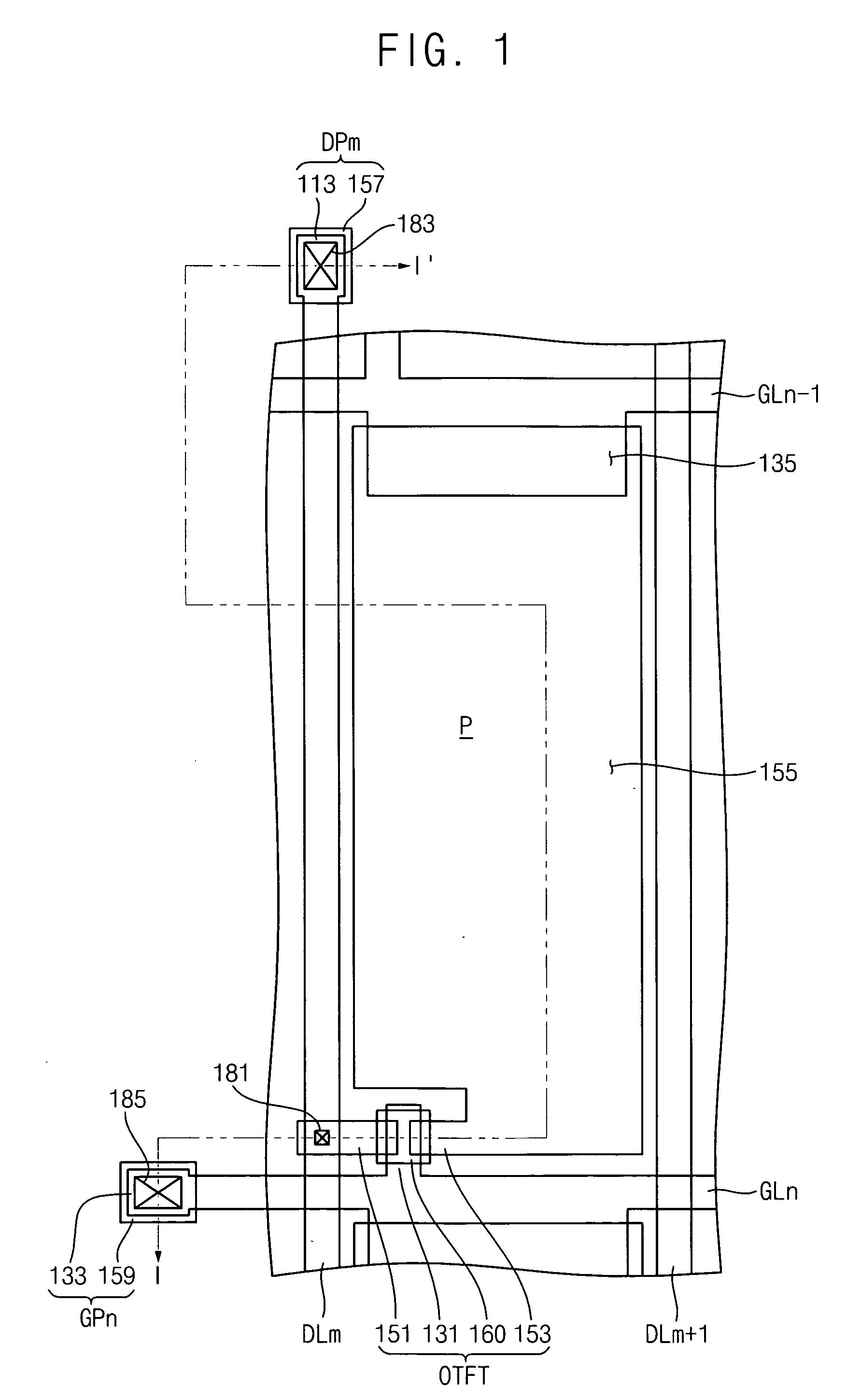
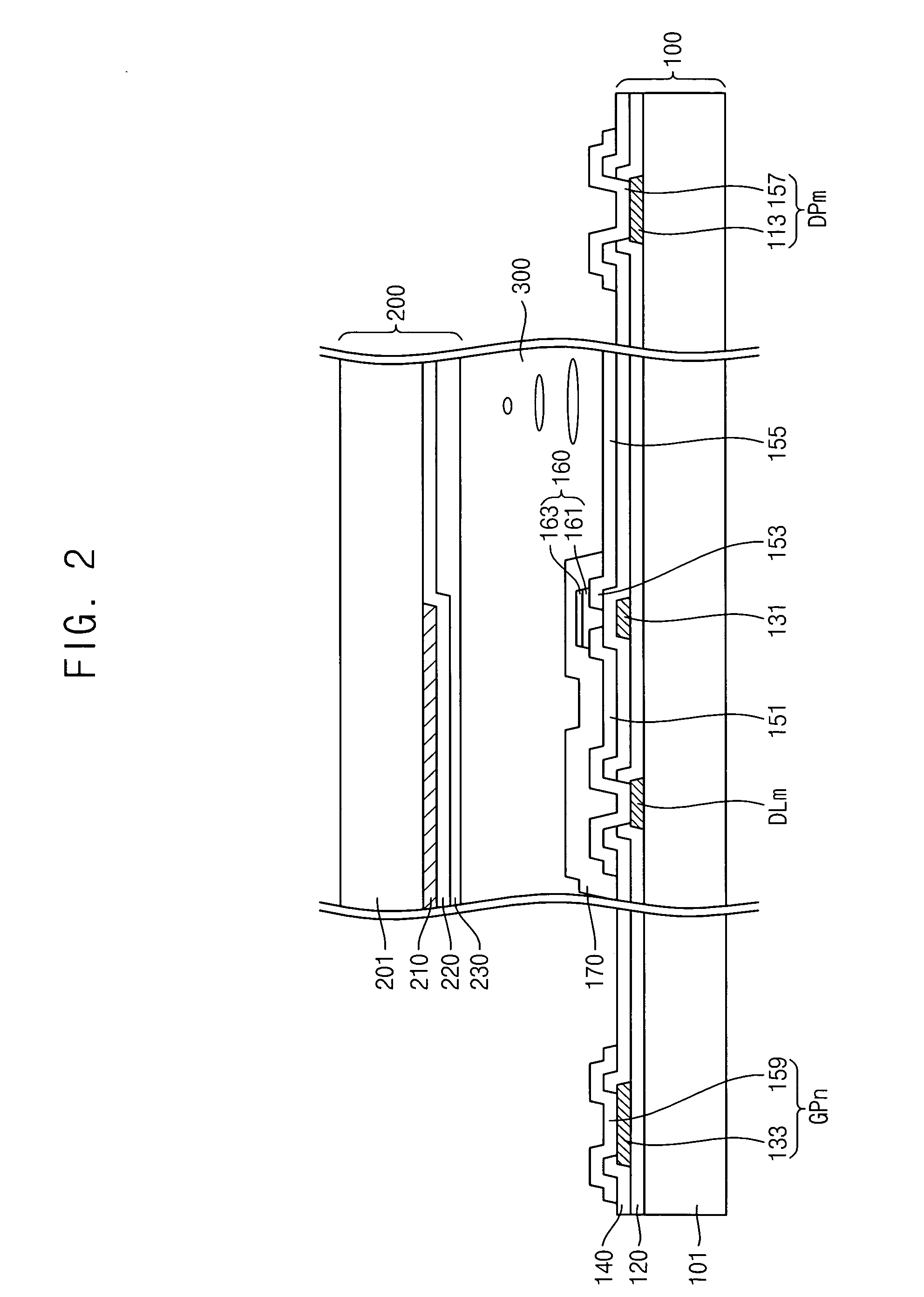
[0022]FIG. 1 is a plan view of a display substrate according to an embodiment of the present invention. The display substrate includes a plurality of data lines DLm and DLm+1 oriented in a longitudinal direction, and a plurality of gate lines GLn-1 and GLn oriented in a transverse direction that crosses the longitudinal direction. Data lines DLm and DLm+1 and gate lines GLn-1 and GLn define pixels P. Each pixel P includes a pixel electrode 155, an organic thin film transistor OTFT, and a storage capacitor electrode 135.

[0023] End portions of data lines DLm and DLm+1 include data pad regions for receiving applied data signals. End portions of gate lines GLn-1 and GLn include gate pad regions for receiving applied gate signals. For example, a data pad DPm is formed at the end of data line DLm, and a gate pad GPn is formed at the end of gate line GLn.

[0024] Data lines DLm and DLm+1 and gate lines GLn-1 and GLn may include copper (Cu), copper alloys, aluminum (Al), aluminum alloys, si...


PUM


Abstract

An improved display substrate is provided to reduce surface defects on insulating layers of organic thin film transistors. Related methods of manufacture are also provided. In one example, a display substrate includes a base, a plurality of data lines, a plurality of gate lines, a pixel defined by the data lines and the gate lines, an organic thin film transistor, and a pixel electrode. The data lines are on the base and are oriented in a first direction. The gate lines are oriented in a second direction that crosses the first direction. The organic thin film transistor includes a source electrode electrically connected to one of the data lines, a gate electrode electrically connected to one of the gate lines, and an organic semiconductor layer. The pixel electrode is disposed in the pixel and electrically connected to the organic thin film transistor. The pixel electrode comprises a transparent oxynitride.

Description

CROSS-REFERENCE TO RELATED APPLICATION [0001] This application claims priority to Korean Patent Application No. 2005-131918, filed in the Korean Intellectual Property Office, Republic of Korea, on Dec. 28, 2005, the disclosure of which is incorporated herein by reference in its entirety. BACKGROUND [0002] 1. Field of the Invention [0003] The present invention relates generally to a display substrate, a method of fabricating the same, and a display panel having the same. More particularly, the present invention relates to a display substrate for liquid crystal displays (LCDs). [0004] 2. Description of Related Art [0005] Liquid crystal displays (LCDs) are one of the most widely used types of flat panel displays. An LCD includes two substrates provided with field-generating electrodes and a liquid crystal (LC) layer interposed therebetween. The LCD displays images by applying voltages to the field-generating electrodes to provide an electric field in the LC layer, which determines orie...

Claims


Application Information

Patent Timeline
IPC IPC(8): H01L29/04H01L29/10
CPCG02F1/13439H01L27/283H01L51/102H01L51/0545H01L51/0541H10K19/10H10K10/464H10K10/466H10K10/82G02F1/136G02F1/355G02F1/361
Inventor LEE, JE-HUNKIM, YOUNG-MINKIM, BO-SUNGLEE, JUN-YOUNGKANG, SUNG-WOOK
Owner SAMSUNG DISPLAY CO LTD
Features
  • Generate Ideas
  • Intellectual Property
  • Life Sciences
  • Materials
  • Tech Scout
  • Unparalleled Data Quality
  • Higher Quality Content
  • 60% Fewer Hallucinations
Learn More