Method for fabricating capacitor

a capacitor and capacitor body technology, applied in the direction of capacitors, semiconductor devices, electrical equipment, etc., to achieve the effect of reducing the bottom area and reducing the improper etching

Inactive Publication Date: 2007-08-30
SK HYNIX INC
View PDF1 Cites 2 Cited by
  • Summary
  • Abstract
  • Description
  • Claims
  • Application Information

AI Technical Summary

Benefits of technology

[0006]A specific embodiment of the present invention is directed to provide a method for fabricating a capacitor in a semiconductor device advantageous for achieving an intended level of capacitance by reducing an improper etching and a decreasing bottom area of an opening region when forming the opening region where a bottom electrode is to be formed.

Problems solved by technology

However, despite this developmental trend, capacitors need to have a minimum level of capacitance to drive semiconductor devices.

Method used


Image

  • Method for fabricating capacitor
  • Method for fabricating capacitor
  • Method for fabricating capacitor

Examples


Embodiment Construction

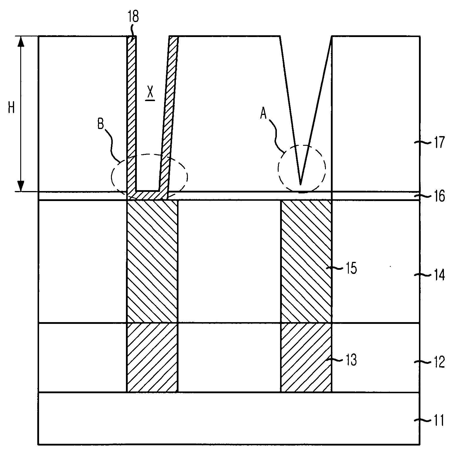
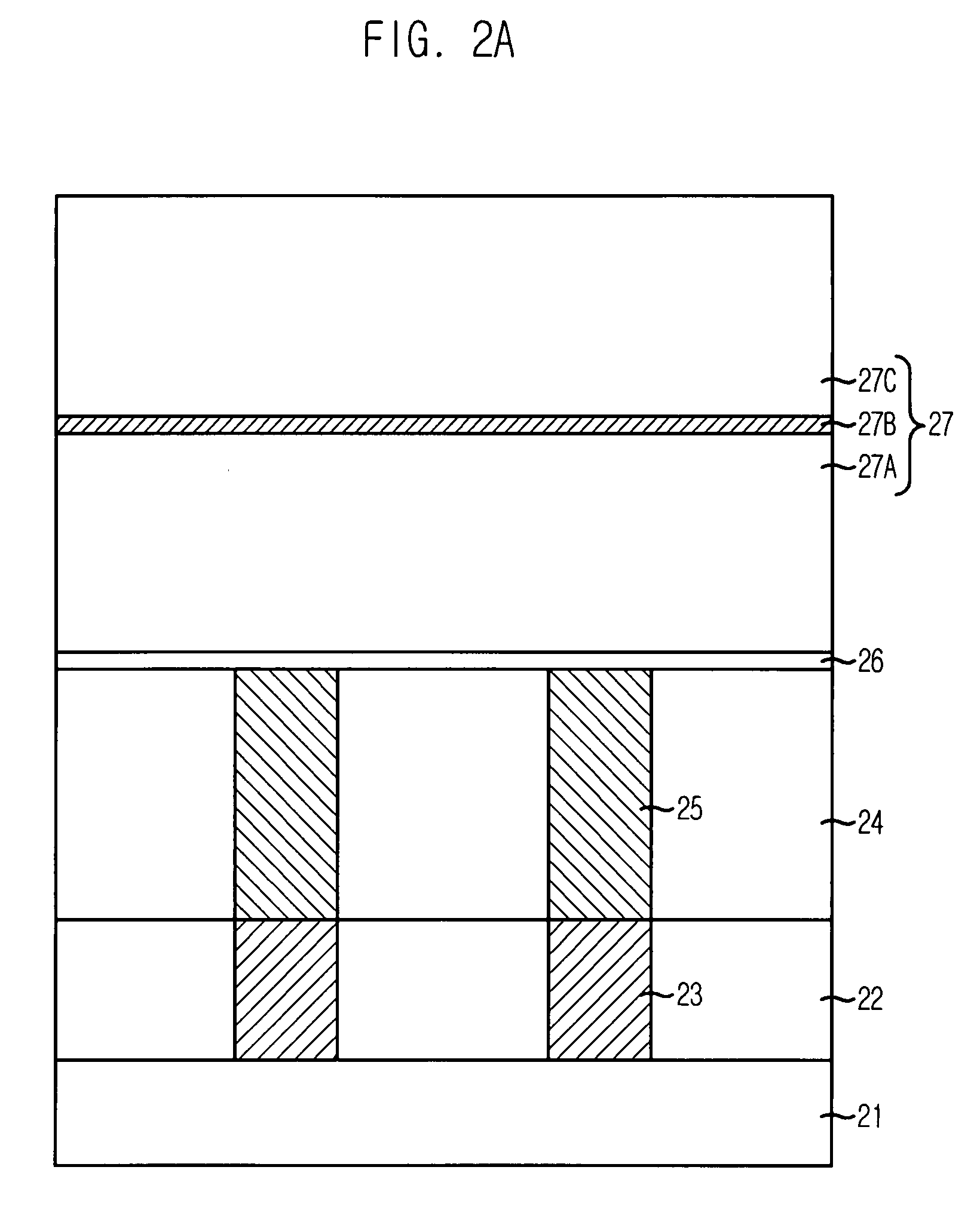
[0012]FIGS. 2A to 2F are sectional views to illustrate a method for fabricating a capacitor in accordance with an embodiment of the present invention. Referring to FIG. 2A, a first insulation layer 22 is formed over a substrate 21, and first contact plugs 23 (e.g., landing contact plugs) passing through the first insulation layer 22 are formed over the substrate 21. In detail, although not illustrated, the first insulation layer 22 is etched to form contact holes. A polysilicon layer is formed over the first insulation layer 22, filling the contact holes, and is etched to form the first contact plugs 23 inside the contact holes. Prior to forming the first contact plugs 23, although not illustrated, transistors may be formed.

[0013]A second insulation layer 24 is formed over the first insulation layer 22 and the first contact plugs, and etched to form other contact holes (not shown). Second contact plugs 25 (e.g., storage node contact plugs) fill the other contact holes. In detail, al...


PUM


Abstract

A method for fabricating a semiconductor device includes forming an insulation structure over a substrate structure including contact plugs, etching the insulation structure to form opening regions each of which has a lower opening portion having a critical dimension wider than an upper opening portion, and forming a conductive layer contacting the contact plugs inside the opening regions.

Description

CROSS-REFERENCES TO RELATED APPLICATIONS[0001]The present invention claims priority of Korean patent application numbers 10-2006-0019612 and 10-2006-0120002, respectively filed on Feb. 28, 2006 and Nov. 30, 2006, respectively, which are incorporated by reference in their entirety.BACKGROUND OF THE INVENTION[0002]The present invention relates to a method for fabricating a semiconductor device, and more particularly, to a method for fabricating a capacitor in a semiconductor device.[0003]As semiconductor devices are being developed toward large-scale of integration, miniaturization and high-speed, areas for capacitors are decreasing. However, despite this developmental trend, capacitors need to have a minimum level of capacitance to drive semiconductor devices. Recently, as semiconductor devices are being scaled down to several nanometers, the height of an inter-layer where capacitors are to be formed increases to secure the capacitance of capacitors.[0004]FIG. 1 is a sectional view t...

Claims


Application Information

Patent Timeline
Patent Type & Authority Applications(United States)
IPC IPC(8): H01L21/4763
CPCH01L28/91H01L21/31116H01L27/04H10B12/00
Inventor HAN, KY-HYUN
Owner SK HYNIX INC
Why Eureka
Try Eureka