Output buffer with switchable output impedance

a buffer and output impedance technology, applied in the field of output buffers, can solve the problems of increasing the power consumption of the dimm, affecting the operation of the input/output buffer, and affecting the operation of the input buffer, so as to avoid undesirable power consumption and reduce power dissipation

Active Publication Date: 2007-09-20
MARVELL ASIA PTE LTD
View PDF8 Cites 76 Cited by
  • Summary
  • Abstract
  • Description
  • Claims
  • Application Information

AI Technical Summary

Benefits of technology

[0011] An output buffer with a switchable output impedance is presented which overcomes the problems noted above, by reducing power dissipation that would otherwise arise due the termination resistor on a signal line being driven, as well as avoiding undesirable power consumption by signal line receivers such as those found in DRAM chips.

Problems solved by technology

The use of termination resistors in this way can have an undesirable side effect, however, in that they tend to increase the DIMM's power consumption.
However, this solution may give rise to another problem, which is illustrated in FIGS. 1b and 1c.
This causes the power consumption of each DRAM line receiver to spike, resulting in a total power consumption which may be unacceptably high.

Method used


Image

  • Output buffer with switchable output impedance
  • Output buffer with switchable output impedance
  • Output buffer with switchable output impedance

Examples


Embodiment Construction

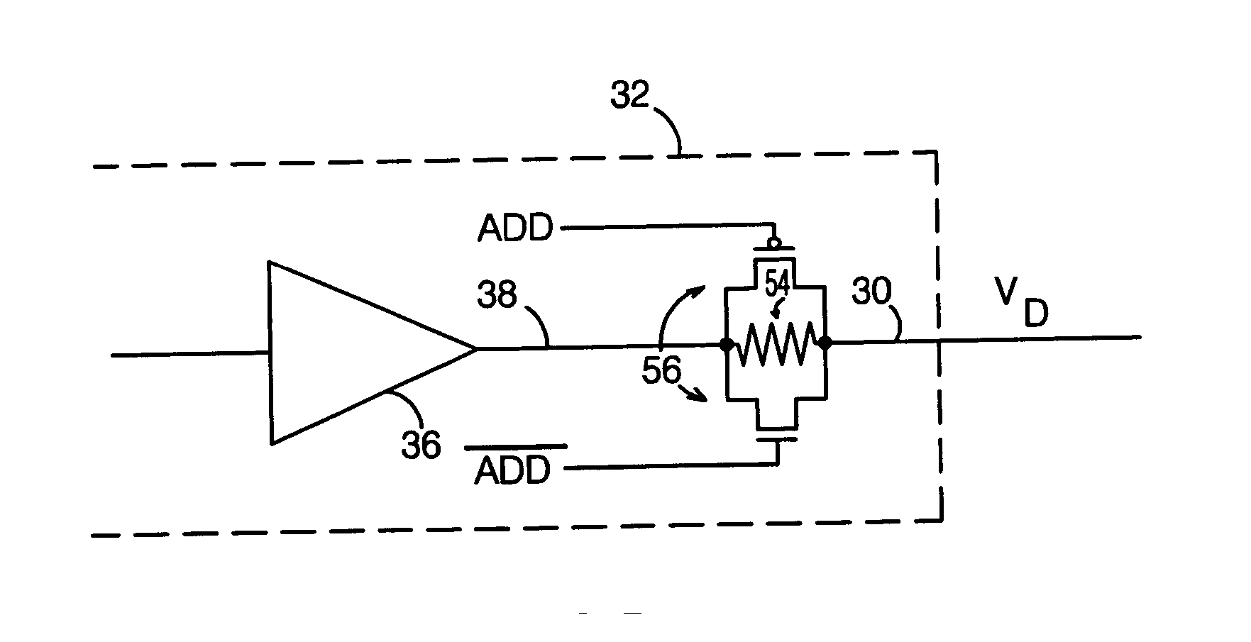
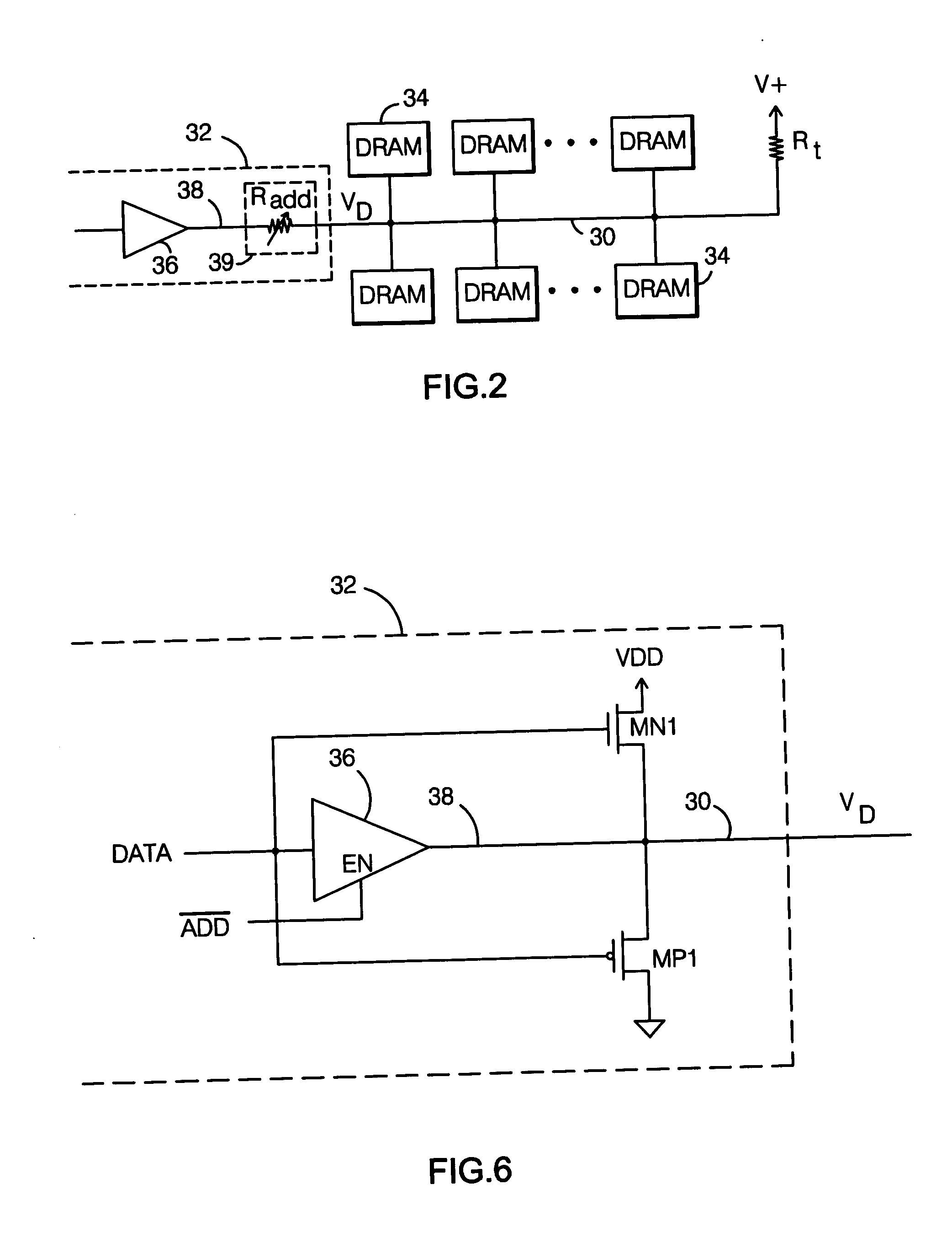
[0023] The present output buffer with switchable output impedance is intended for use driving terminated signal lines, particularly when power consumption is a concern. By controlling the buffer's output impedance, the power consumption of a system employing the buffer can be reduced in comparison with systems which lack this capability.

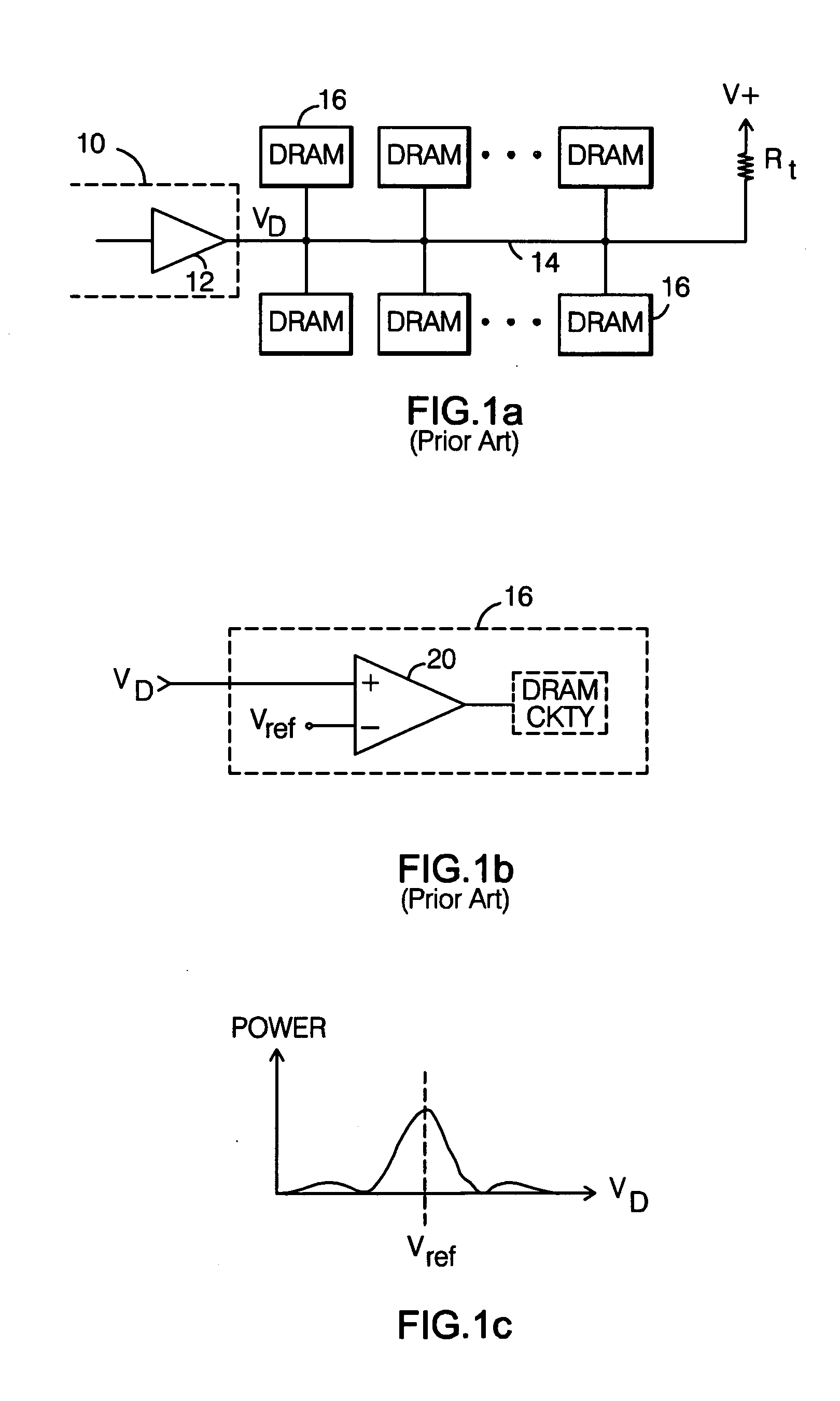
[0024] Though the present buffer is generally applicable to any terminated signal line application, a primary application is in a memory system, in which each buffer drives a respective terminated address or control line routed to multiple RAM chips populating a DIMM memory module. For example, for DIMMs in compliance with the DDR3 specifications promulgated by JEDEC, each address and control line is routed to multiple DRAM chips on the DIMM, and each line is terminated with a termination resistor having a resistance Rt. For purposes of illustration, this application is described throughout, though the invention is in no way limited to use with DIMM...


PUM


Abstract

An output buffer with a switchable output impedance designed for driving a terminated signal line. The buffer includes a drive circuit, and a means for switching the output impedance of the drive circuit between a first, relatively low output impedance when the output buffer is operated in a ‘normal’ mode, and a second output impedance which is greater than the first output impedance when operated in a ‘standby’ mode. By increasing the drive circuit's output impedance while in ‘standby’ mode, power dissipation due to the termination resistor is reduced. When used in a memory system, additional power savings may be realized by arranging the buffer such that the increased impedance in ‘standby’ mode shifts the signal line voltage so as to avoid the voltage range over which a line receiver's power consumption is greatest.

Description

BACKGROUND OF THE INVENTION [0001] 1. Field of the Invention [0002] This invention relates to the field of output buffers, and particularly to output buffers used to drive terminated signal lines. [0003] 2. Description of the Related Art [0004] There are many applications in which output buffers drive respective signal lines to convey data to one or more devices connected to the signal lines. In such applications, it is important that the integrity of the data on the signal lines be maintained, so that it can be accurately detected by the receiving devices. [0005] One such application is a random access memory (RAM) system. Dual-Inline Memory Modules (DIMMs) are the industry-standard platform on which RAM is provided for digital computers. Each DIMM is a printed-circuit board which contains a number of individual RAM integrated circuits (ICs) or “chips.” DIMMs typically contain address and / or control registers which distribute data bits to each of the DIMM's RAM chips via signal lin...

Claims


Application Information

Patent Timeline
Patent Type & Authority Applications(United States)
IPC IPC(8): H03K19/094
CPCH03K19/0005H03K19/094H03K19/018557
Inventor RAGHAVAN, GOPALJAIN, DHRUV
Owner MARVELL ASIA PTE LTD
Why Eureka
Try Eureka