

Nano-electrode-array for integrated circuit interconnects
a technology of integrated circuits and electron arrays, applied in the field of semiconductor technology, can solve the problems of reducing the advantage of using high conductivity materials, short circuits in integrated circuits, and uniform thickness of very thin layers of integrated circuits
- Summary
- Abstract
- Description
- Claims
- Application Information
AI Technical Summary
Problems solved by technology
Method used
Image

Examples
Embodiment Construction
[0037] In the following description, numerous specific details are given to provide a thorough understanding of the invention. However, it will be apparent that the invention may be practiced without these specific details. In order to avoid obscuring the present invention, some well-known circuitry and process steps are not disclosed in detail.
[0038] Likewise, the drawings showing embodiments of the transistor are semi-diagrammatic and not to scale and, particularly, some of the dimensions are for the clarity of presentation and are shown greatly exaggerated in the FIGs.
[0039] In addition, where multiple embodiments are disclosed and described having some features in common, for clarity and ease of illustration, description, and comprehension thereof, similar and like features one to another will ordinarily be described with like reference numerals.
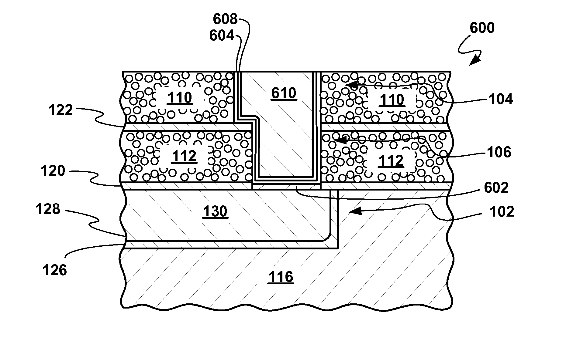
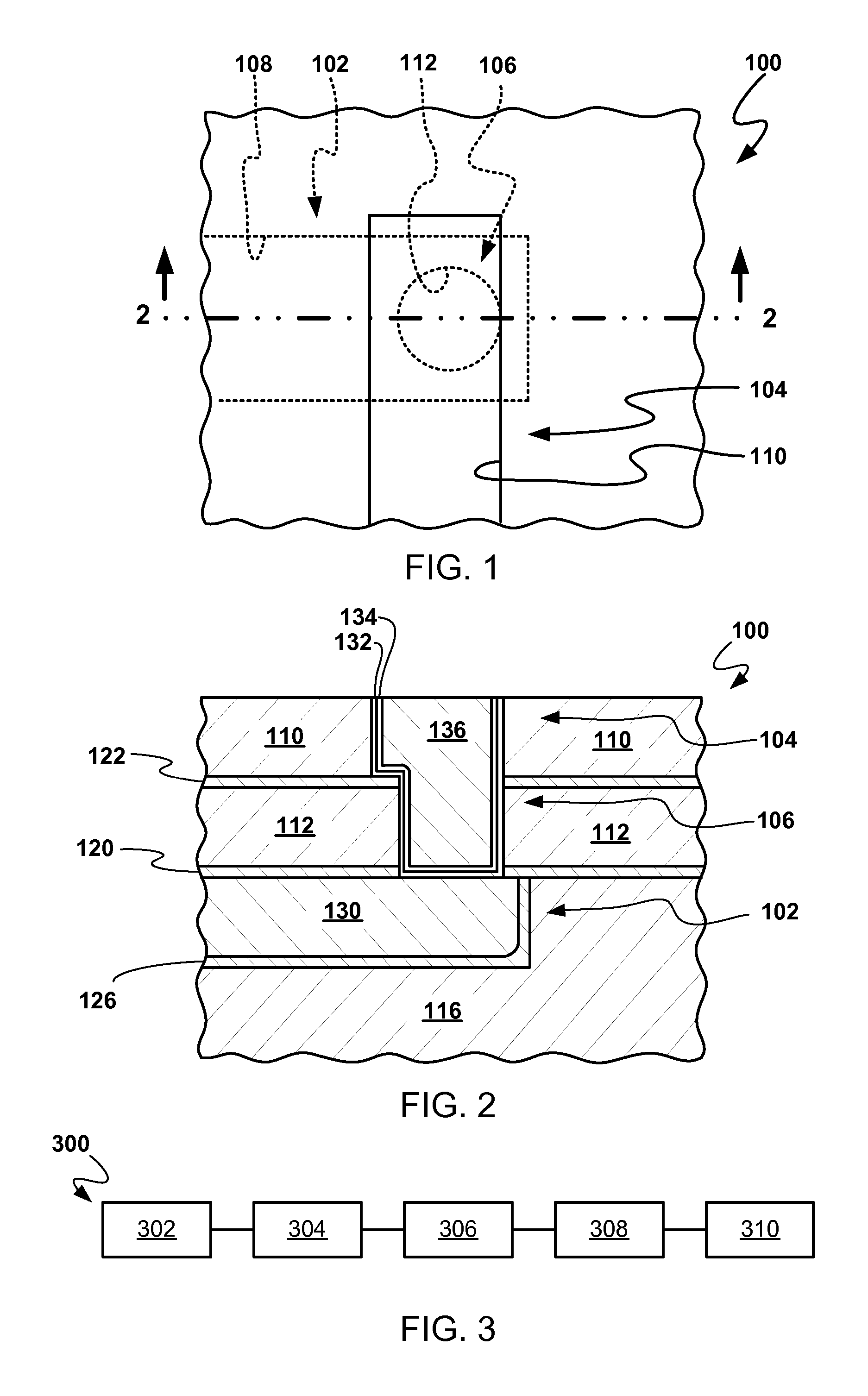
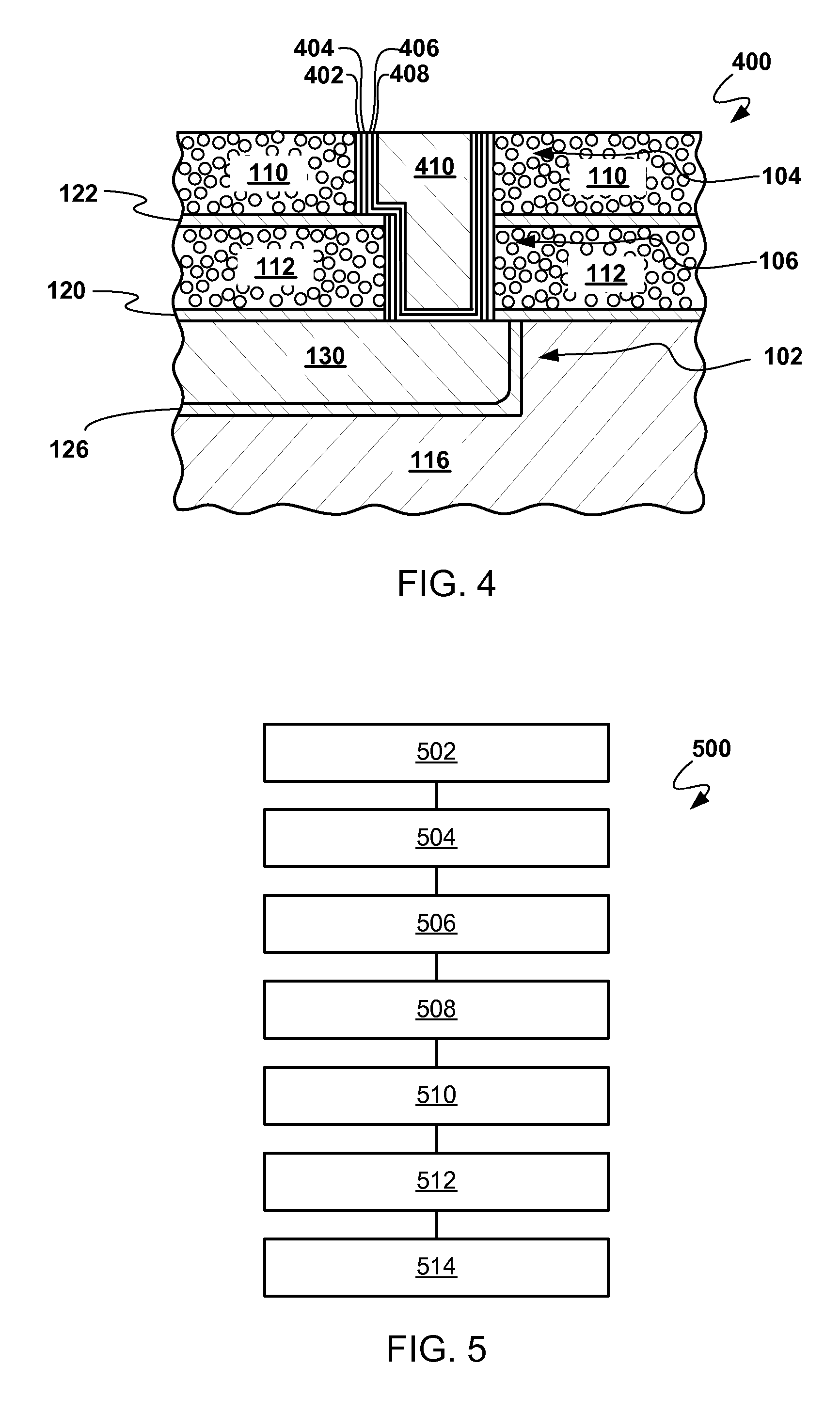
[0040] Referring now to FIG. 1, therein is shown a plan view of an integrated circuit 100 in accordance with an embodiment of the pr...
PUM
 Abstract
Description
Claims
Application Information