
Nanostructure Assemblies, Methods And Devices Thereof

a technology of nanostructures and assemblies, applied in the field of nanostructures, can solve the problems of inability to fully understand the assembly process of nanostructures such as ncs, small arrays of nc qds, and system of two nc qds with independently controllable qds,

Active Publication Date: 2008-01-24
THE TRUSTEES OF THE UNIV OF PENNSYLVANIA
View PDF46 Cites 137 Cited by
  • Summary
  • Abstract
  • Description
  • Claims
  • Application Information

AI Technical Summary

Benefits of technology

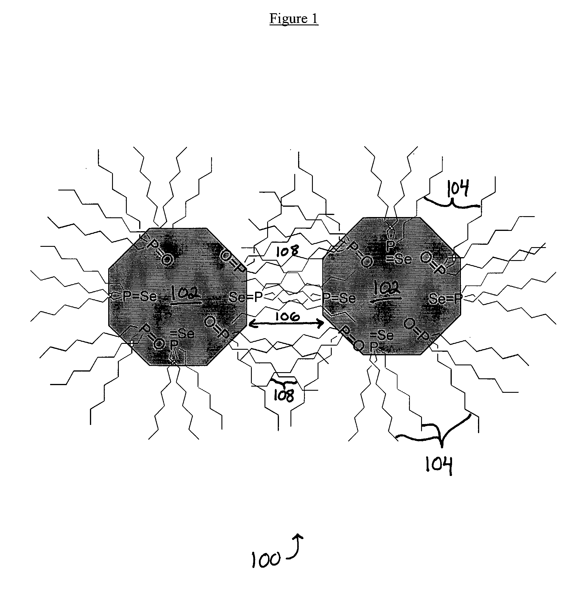
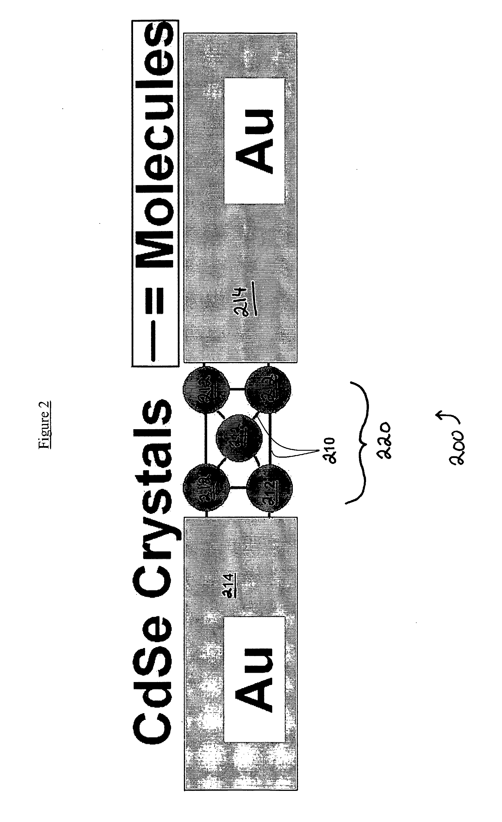
[0013] The present invention also provides nanocrystal arrays comprising at least two molecularly bridged nanocrystals, as well as field effect transistors comp

Problems solved by technology

Although Brus and co-workers [24] have analyzed the drying-mediated self-assembly of nanoparticles using models of homogeneous and non-homogeneous solvent evaporation, the assembly process of nanostructures such as NCs is not fully understood.
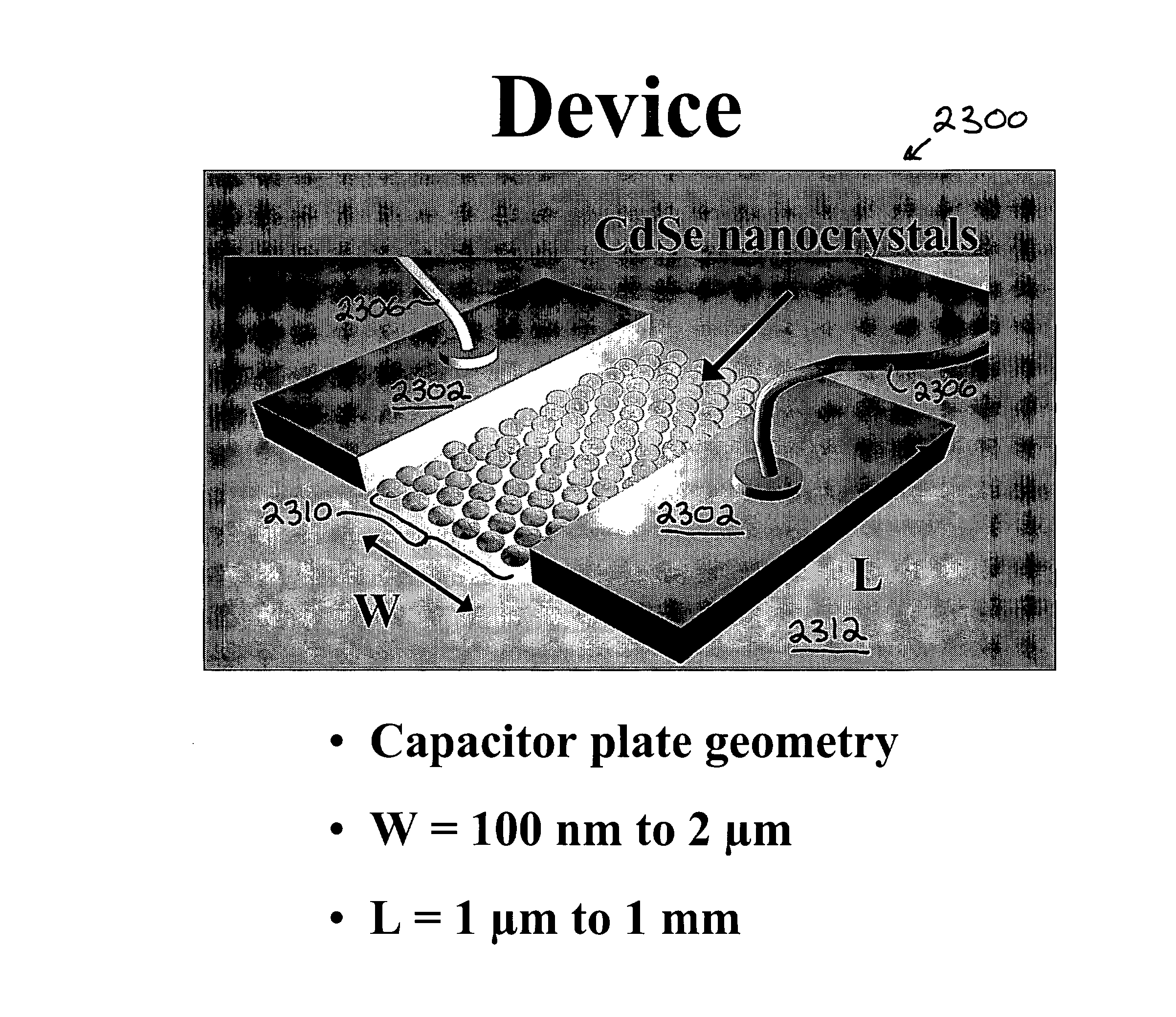
However, small arrays of NC QDs, for example, a system of two NC QDs with independently controllable QDs, has not been achieved yet.

Method used


Image

  • Nanostructure Assemblies, Methods And Devices Thereof
  • Nanostructure Assemblies, Methods And Devices Thereof
  • Nanostructure Assemblies, Methods And Devices Thereof

Examples


Embodiment Construction

[0058] The present invention may be understood more readily by reference to the following detailed description taken in connection with the accompanying figures and examples, which form a part of this disclosure. It is to be understood that this invention is not limited to the specific devices, methods, conditions or parameters described and / or shown herein, and that the terminology used herein is for the purpose of describing particular embodiments by way of example only and is not intended to be limiting of the claimed invention. Also, as used in the specification including the appended claims, the singular forms “a,”“an,” and “the” include the plural, and reference to a particular numerical value includes at least that particular value, unless the context clearly dictates otherwise. When a range of values is expressed, another embodiment includes from the one particular value and / or to the other particular value. Similarly, when values are expressed as approximations, by use of t...


PUM


Abstract

Disclosed herein are methods for assembling nanostructures. The assembling methods include contacting the plurality of nanostructures to a substrate having one or more discontinuities. At least a portion of the plurality of nanostructures assemble adjacent to the discontinuity, the assembled nanostructures including at least one nanostructure having a bridging, molecule. Devices, such as field-effect transistors, are also disclosed.

Description

CROSS REFERENCE TO RELATED APPLICATIONS [0001] This application claims the benefit of U.S. Provisional Application Ser. No. 60 / 574,352, filed May 25, 2004, the entirety of which is incorporated by reference herein. This application also claims the benefit of U.S. Provisional Application Ser. No. 60 / 663,637, filed Mar. 21, 2005, the entirety of which is incorporated by reference herein.STATEMENT OF GOVERNMENT RIGHTS [0002] The invention was made with U.S. Government support. The Government may have certain rights in the invention under Office of Naval Research Grant No. N000140410489 and NSF IGERT Program Grant No. DGE-0221664.FIELD OF THE INVENTION [0003] The field of the invention generally relates to nanostructures, processes for manipulating nanostructures, and devices prepared using nanostructures. BACKGROUND OF THE INVENTION [0004] Interesting quantum effects occur when electrons are confined in small regions, such as in nanostructures, examples of which include quantum dots (“...

Claims


Application Information

Patent Timeline
IPC IPC(8): H01L29/24H01L21/336H01L29/78H01L51/00
CPCB82B3/00B82Y10/00B82Y30/00B82Y40/00H01L29/7613Y10T428/25H01L51/0052H01L51/0595H01L51/102Y10T428/26H01L51/0048H10K85/221H10K85/615H10K10/701H10K10/82
Inventor DRNDIC, MARIJAFISCHBEIN, MICHAEL D.
Owner THE TRUSTEES OF THE UNIV OF PENNSYLVANIA
Learn More