Chip-scale coils and isolators based thereon

a technology of isolators and coils, applied in the field of coils, can solve the problems of affecting the cost of manufacturing an isolator, and essentially waste of the die area, so as to improve transformer performance, reduce the capacitance of coils, and reduce the loss of substrates

Inactive Publication Date: 2008-02-07
ANALOG DEVICES INC
View PDF90 Cites 29 Cited by
  • Summary
  • Abstract
  • Description
  • Claims
  • Application Information

AI Technical Summary

Benefits of technology

[0015] This arrangement allows the substrate supporting the coil(s) to be made of an insulating material such as a glass, rather than a semiconductor material. In this way, when the field-receiving element is a coil, forming a transformer with the field-generating coil, improved transformer performance is obtainable. That is, such transformers are well-suited for dual direction, symmetrical drive / receive operation. Coil-substrate capacitance is reduced, there is less substrate loss and other parameters, such as creepage, are improved.

Problems solved by technology

Despite the benefits of the foregoing isolator designs, with respect to the coil-type isolator, manufacturing costs are still higher than is desired in many situations.
Since cost is a direct function of die area requirements, coil size thus strongly influences the cost of manufacturing an isolator.
Additionally, many of the expensive semiconductor processing steps used to create the input and / or output circuitry are unnecessary for coil fabrication and are essentially wasted on most of the die area.
At the same time, some of the coil fabrication steps, usually performed in “post processing” operations after the circuitry is created, may be deleterious to the circuitry so the circuitry must be protected during coil manufacture.
Further, some of the processing methods which desirably would be used to fabricate the coils could, in fact, be problematic when the coils and circuitry are on the same substrate.
Consequently, other, less desirable methods have to be used to fabricate the coils when input and / or output circuitry is made on the same substrate with the coils.

Method used


Image

  • Chip-scale coils and isolators based thereon
  • Chip-scale coils and isolators based thereon
  • Chip-scale coils and isolators based thereon

Examples


Embodiment Construction

[0039] As this invention improves upon that shown in U.S. patent application Ser. No. 09 / 838,520, we shall first review appropriate portions of the disclosure from that application. Some of those portions relate to isolators which use elements other than coils to establish the isolation barrier, but they show input and output circuitry and signals usable with transformer-based isolators, as well.

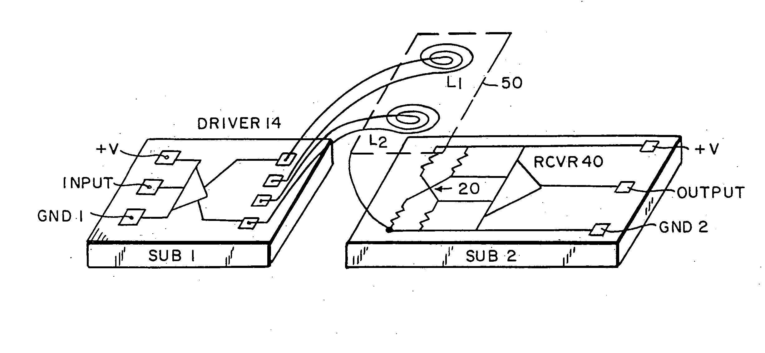
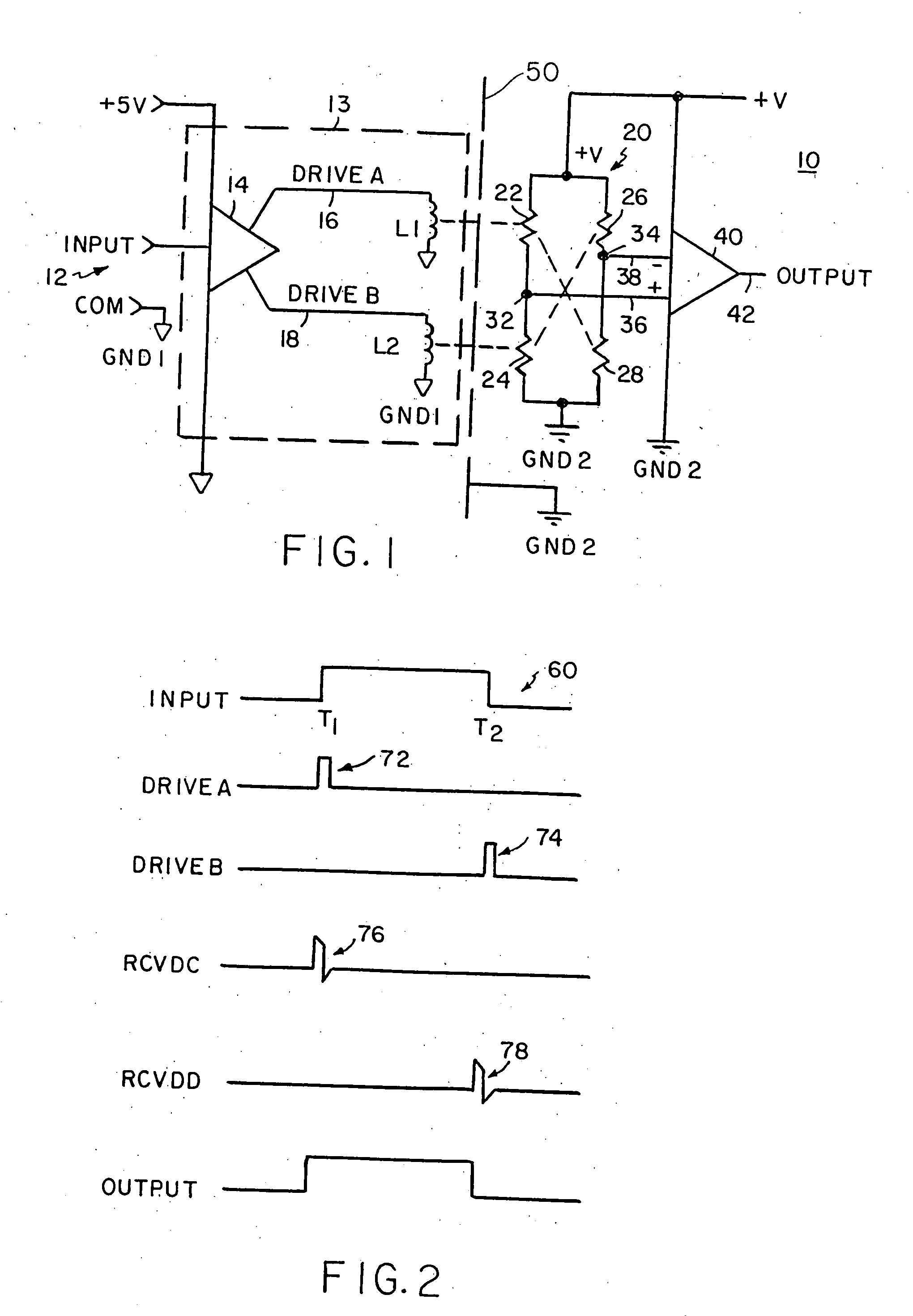
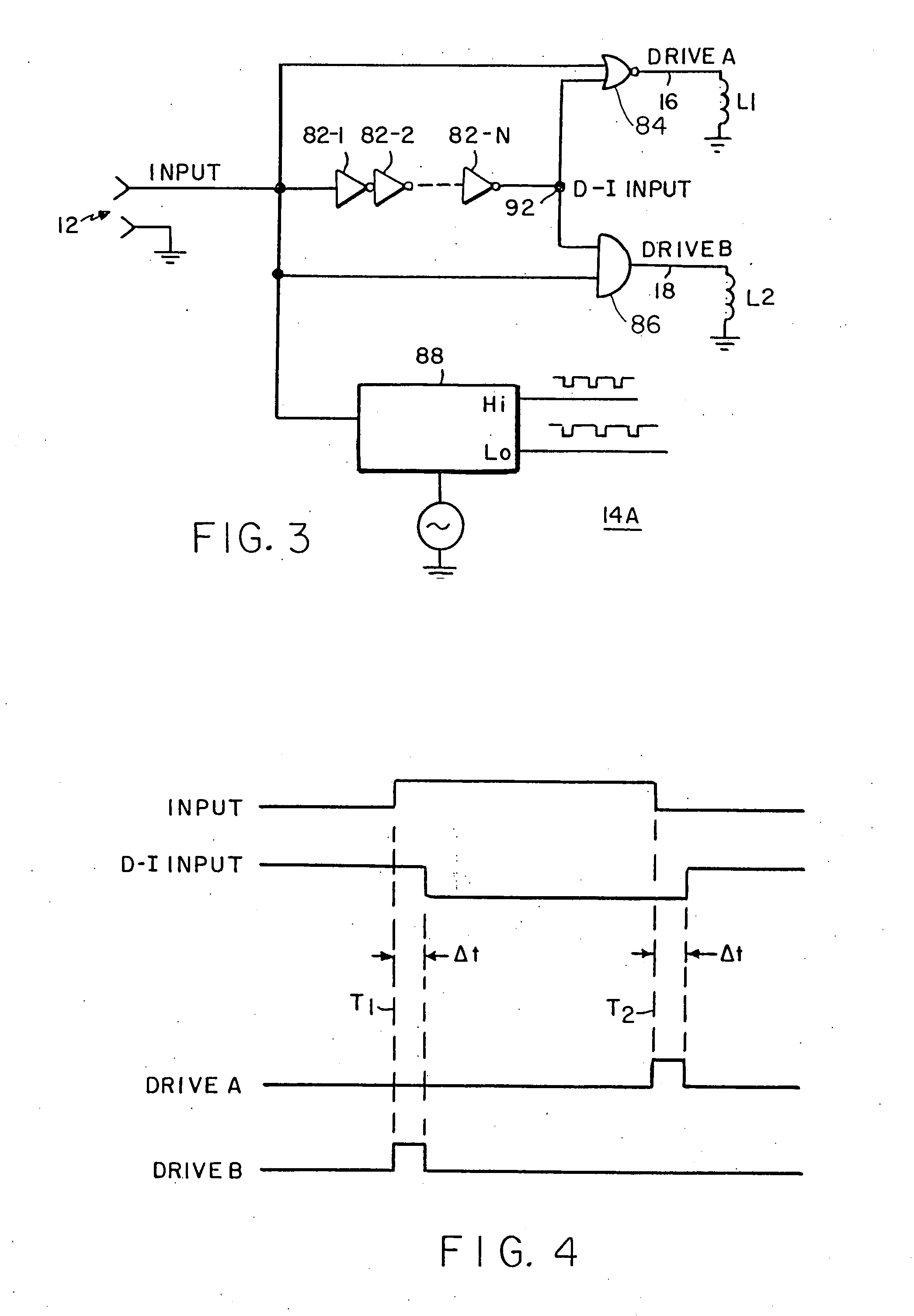
[0040] An exemplary implementation of an isolator 10 using coil-type field-generating and MR field-sensing (receiving) elements is illustrated schematically in FIG. 1. An input voltage is supplied at port 12 to a magnetic field generator 13, comprising an input driver 14 and one or more coils L1, L2. Driver 14 supplies output signals DRIVE A and DRIVE B on lines 16 and 18, respectively, to respective coils L1 and L2. Each of coils L1 and L2 generates a magnetic field which is sensed by a bridge 20 formed by MR elements 22, 24, 26 and 28. Elements 22 and 24 are connected in series across the...


PUM

PropertyMeasurementUnit
resistivityaaaaaaaaaa
dielectricaaaaaaaaaa
magnetic fieldaaaaaaaaaa

Abstract

Coil structures and isolators using them. A coil(s) is (are) used as a magnetic field-generating element(s) paired with another coil(s) or other magnetic field-receiving element(s). The coil(s) is(are) formed in or on a substrate which does not include some or all of the driver (i.e., input) or receiver (i.e., output) circuits. The coil(s) and magnetic field-receiving element(s) thus can be manufactured separately from the driver and/or receiver circuitry, using different processes, instead of subjecting the chip areas containing both input and output circuits to post processing to form the coil(s). Isolators can be assembled using such coils with a resultant lower cost. Isolators also can be assembled using transformers made from such coils wherein the transformers can be driven on either of their windings in order to provide bi-directional isolation with a single transformer.

Description

CROSS-REFERENCE TO RELATED APPLICATIONS [0001] This application is a continuation of U.S. patent application Ser. No. 10 / 214,883, filed Aug. 8, 2002, which is a continuation-in-part of Ser. No. 09 / 838,520, filed Apr. 19, 2001, which is a continuation-in-part of Ser. No. 09 / 557,542, filed Apr. 25, 2000, which is a continuation of Ser. No. 09 / 118,032, filed Jul. 17, 1998, now U.S. Pat. No. 6,054,780, which claims priority from provisional application No. 60 / 063,221. These priority documents are expressly incorporated by reference for all purposes.FIELD OF THE INVENTION [0002] This invention relates to coils as well as to coil-based or partially coil-based isolator circuitry and structures for isolating electronic signals. Such isolators are used, for example, to interface and galvanically isolate sensor signals in a process control system, or between microcontrollers and other signal sources and transducers or other devices using those signals. BACKGROUND OF THE INVENTION [0003] In a ...

Claims


Application Information

Patent Timeline
Patent Type & Authority Applications(United States)
IPC IPC(8): H04B15/00H01F17/00H01F19/08H01F38/14H01L23/522H01L23/60H04B5/00H04L25/02
CPCH01F17/0006H01F19/08H01L2924/3025H01L2224/49175H01L2224/48137H01F38/14H01F2019/085H01L23/5222H01L23/5227H01L23/60H01L2924/3011H03H7/52H04B5/005H04B5/0093H04L25/0266H01L2224/48091H01L2924/00H01L2924/00014H01L2224/05553H01L2224/45099
Inventor CHEN, BAOXINGKLIGER, RONN
Owner ANALOG DEVICES INC
Why Eureka
Try Eureka