Eureka AIR delivers breakthrough ideas for toughest innovation challenges, trusted by R&D personnel around the world.

Method and apparatus for determining LSI type, method and apparatus for supporting LSI design, and computer product

Inactive Publication Date: 2008-02-28
FUJITSU LTD
View PDF7 Cites 3 Cited by
  • Summary
  • Abstract
  • Description
  • Claims
  • Application Information

AI Technical Summary

Benefits of technology

[0019]A circuit design support apparatus according to another aspect of the present invention includes a receiving unit the receives information from an intermediate product, with respect to each intermediate product, of a structured ASIC having at least a transistor layer; an identifying unit that identif

Problems solved by technology

However, for the above-mentioned conventional technologies, as speed variations in LSI operation result depending on conditions at the time of manufacturing, it is difficult to control the performance of LSI to be manufactured.
For ASIC and structured ASIC, a great deal of time and cost may be required for the timing design to ensure the performance required for the specific application.
In such a case, a design period may be shortened conceivably by using only units that meet performance specifications Since ASIC and structured ASIC, are manufactured specific to an application, units that do not meet performance requirements for the specific application can not be utilized for other applications and hence become useless, resulting in a problem of increased manufacturing cost.
Also, variations in current leakage result depending on the conditions at the time of manufacturing.
However, for a chip with a small current leakage, this selection process results in the use of an unnecessarily expensive package, further resulting in a problem of an increased manufacturing cost.
Furthermore, in LSIs for which there are great restrictions in terms of power consumption and chip unit price for manufacturing, a great deal of time may be spent on the design to satisfy such restrictions, and thereby leading to a problem of a longer design period.
However, a problem with FPGA is that in addition to a high chip unit price, the performance of the LSI that can be manufactured is inferior to that of the ASIC or the structured ASIC.

Method used


Image

  • Method and apparatus for determining LSI type, method and apparatus for supporting LSI design, and computer product
  • Method and apparatus for determining LSI type, method and apparatus for supporting LSI design, and computer product
  • Method and apparatus for determining LSI type, method and apparatus for supporting LSI design, and computer product

Examples


Embodiment Construction

[0034]Exemplary embodiments according to the present invention will be explained in detail below with reference to accompanying drawings.

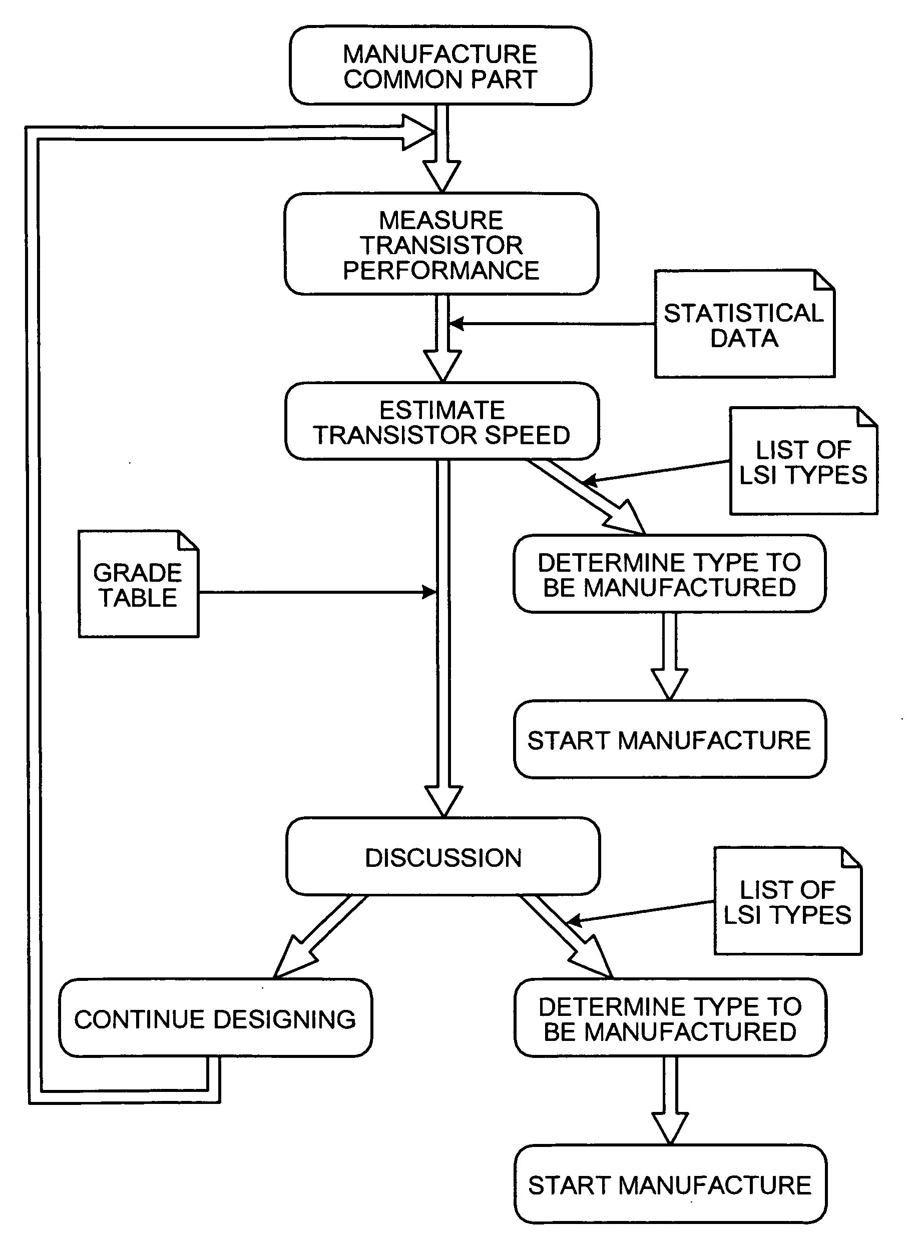
[0035]FIG. 1 is a flow diagram of an LSI design service according to an embodiment of the present invention. In the LSI design service shown in FIG. 1, the manufactured LSI is a structured ASIC.

[0036]Structured ASICs are common in structure up to a transistor layer (or a transistor layer and a metal 1 layer) formed on a silicon wafer, and by varying a wiring layer (metal layer) formed thereon, various operations are obtained. Upon formation of the common transistor layer, performance of the LSI is determined to a certain extent in the structured ASIC.

[0037]In the LSI service shown in FIG. 1, an LSI manufacturer (a vendor) manufactures an intermediate product by forming the transistor layer (or the transistor layer and the metal 1 layer) on the surface of the silicon wafer. The intermediate product as used here may be a disk-shaped (for example, hav...


PUM


Abstract

In manufacturing a structured ASIC, after production of an intermediate product with a transistor layer or the transistor layer and a metal layer, the transistor speed of each intermediate product is measured and, using the speed and associated statistical data, a maximum transistor speed delay is estimated. Based on the estimate, the type of the structured ASIC is determined from among an existing list of LSI circuit types.

Description

CROSS-REFERENCE TO RELATED APPLICATIONS[0001]This application is based upon and claims the benefit of priority from the prior Japanese Patent Application No. 2006-229266, filed on Aug. 25, 2006, the entire contents of which are incorporated herein by reference.BACKGROUND OF THE INVENTION[0002]1. Field of the Invention[0003]The present invention relates to design of a large-scale integration (LSI), such as a structured application specific integrated circuit (ASIC).[0004]2. Description of the Related Art[0005]Conventionally, ASICs, field programmable gate arrays (FPGA) and structured ASICs are available as application specific LSI circuits. The ASIC has transistor and metal layers specific to the type of LSI to be manufactured that formed on the surface of a silicon wafer (e.g., Japanese Patent Application Laid-Open Publication No. H06-29391).[0006]The FPGA is designed to have its logic components (circuit function) configured after manufacturing, thereby enabling a user to change th...

Claims


Application Information

Patent Timeline
IPC IPC(8): G06F17/50
CPCH01L22/14
Inventor KANAZAWA, YUZI
Owner FUJITSU LTD
Why Eureka
Eureka Blog
Learn More