Plasma display panel
a technology of display panel and plasma, which is applied in the direction of address electrodes, static indicating devices, instruments, etc., can solve the problems of increased discharge delay time, increased discharge instability, and increased discharge start voltage and discharge sustain voltage between front substrate electrodes, so as to improve discharge stability, reduce power consumption, and improve brightness and efficiency
- Summary
- Abstract
- Description
- Claims
- Application Information
AI Technical Summary
Benefits of technology
Problems solved by technology
Method used
Image
Examples
first embodiment
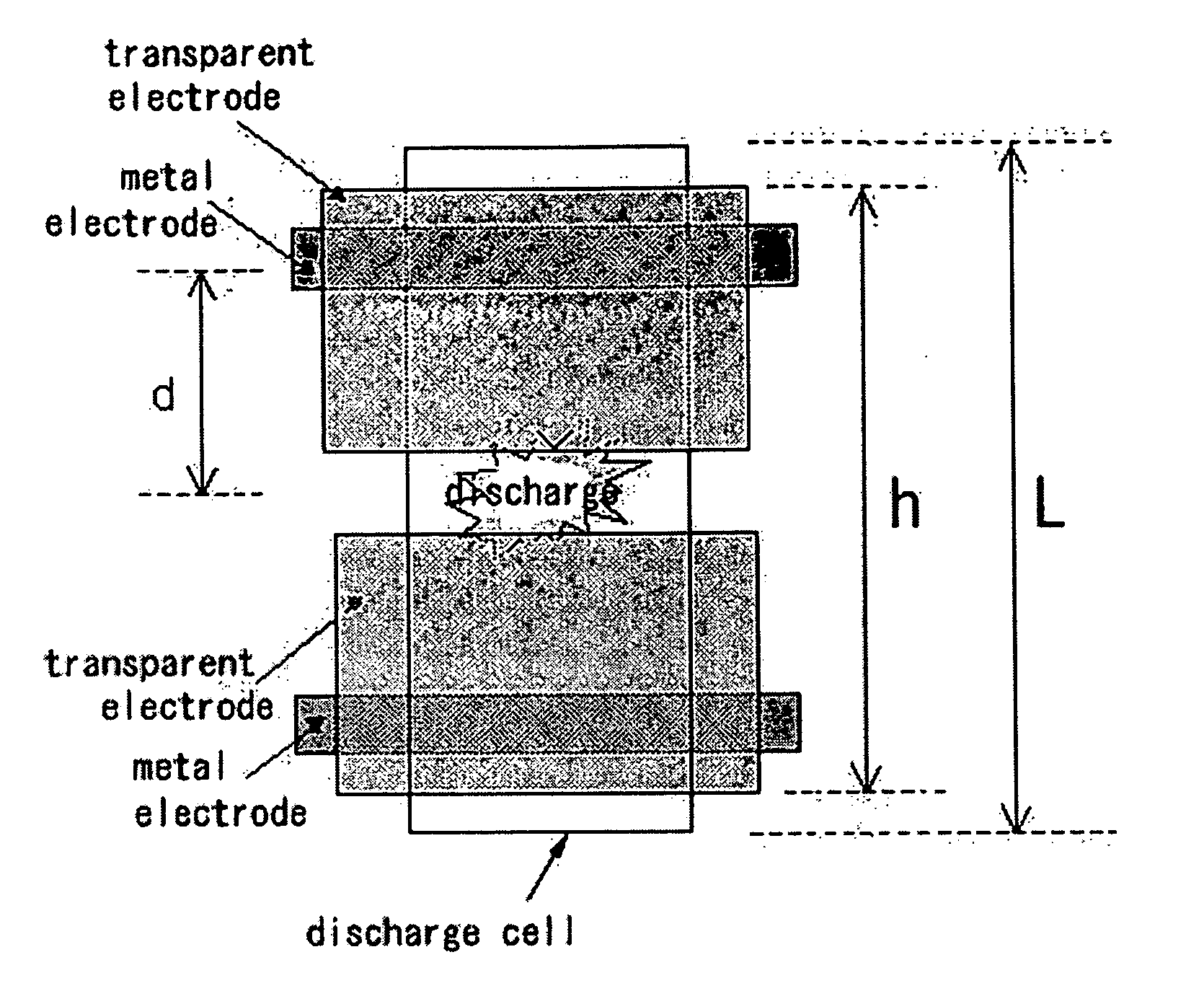
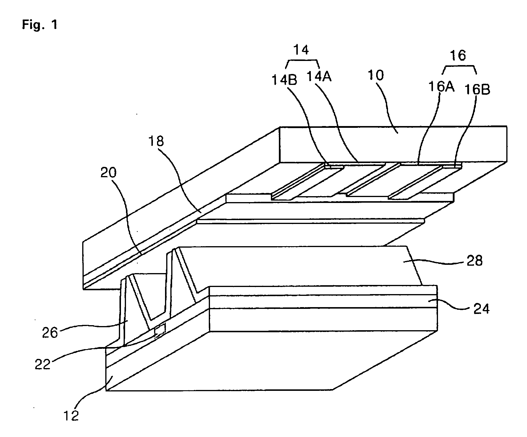
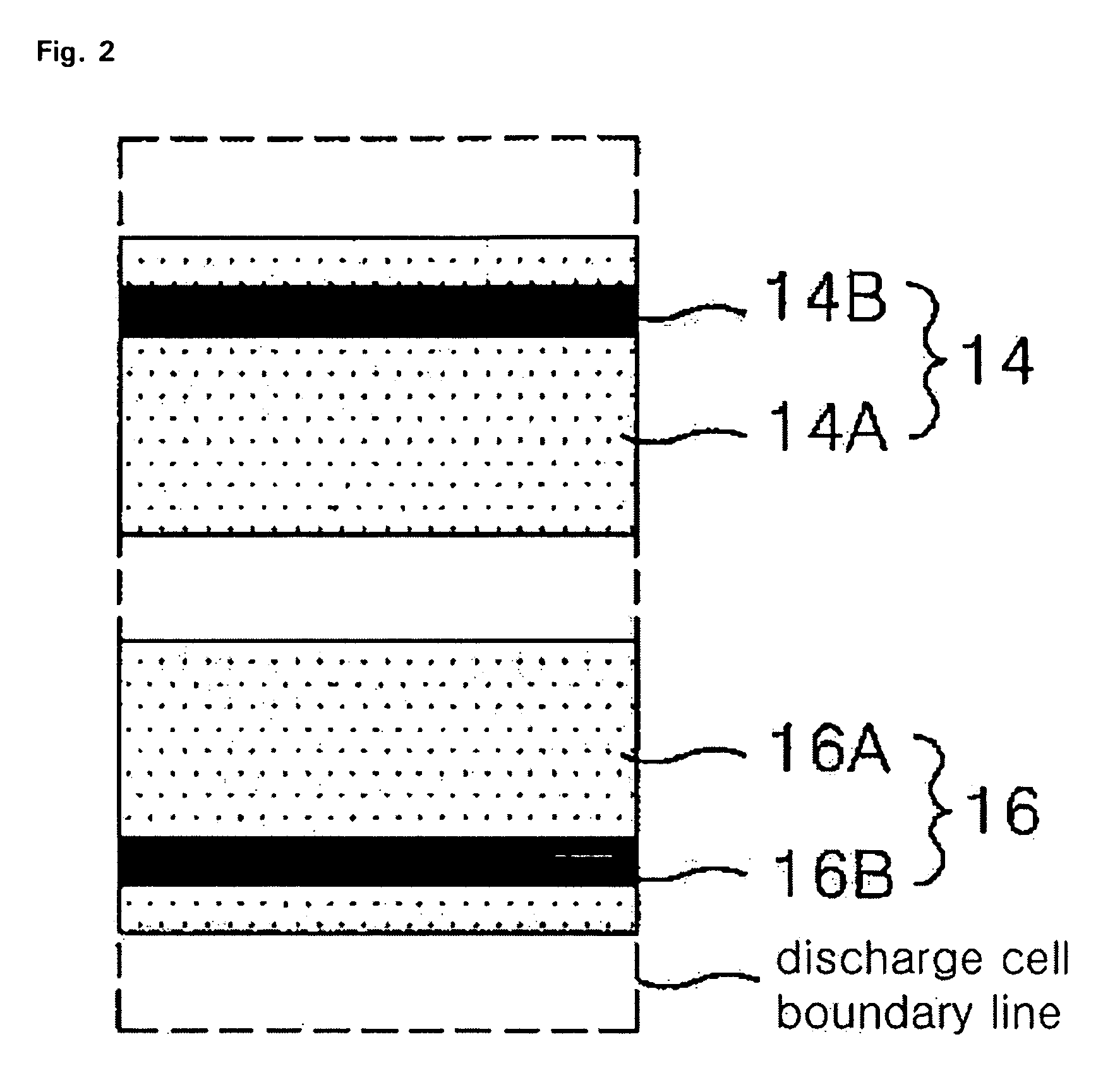
[0059] According to a first embodiment of the present invention, there is provided a plasma display panel having a front substrate and a rear substrate opposite to each other, the plasma display panel including a pair of transparent electrodes formed on the opposite surface of the front substrate, metal electrodes each formed on the transparent electrodes, a dielectric layer that covers the transparent electrodes and the metal electrodes, a protection film coated on the dielectric layer, address electrodes formed on the opposite surface of the rear substrate, a dielectric layer that covers the address electrodes, barrier ribs formed on the dielectric layer, a discharge cell demarcated by the barrier ribs, and a phosphor layer coated on the inside of the discharge cell, wherein assuming that a distance from the center of a discharge region between the pair of the transparent electrodes to the center of the metal electrodes is “d” and a distance between both ends of the pair of the tr...
second embodiment
[0076] According to a second embodiment of the present invention, there is provided a plasma display panel having a front substrate and a rear substrate opposite to each other, the plasma display panel including a pair of transparent electrodes formed on the opposite surface of the front substrate, metal electrodes each formed on the transparent electrodes, a dielectric layer that covers the transparent electrodes and the metal electrodes, a protection film coated on the dielectric layer, address electrodes formed on the opposite surface of the rear substrate, a dielectric layer that covers the address electrodes, barrier ribs formed on the dielectric layer, a discharge cell demarcated by the barrier ribs, and a phosphor layer coated on the inside of the discharge cell, wherein the metal electrodes are formed at locations inclined toward a side where the pair of the transparent electrodes are opposite to each other, and the plasma display panel further comprises auxiliary metal elec...
third embodiment
[0103] According to a third embodiment of the present invention, there is provided a plasma display panel having a front substrate and a rear substrate opposite to each other, the plasma display panel including a pair of transparent electrodes formed on the opposite surface of the front substrate, metal electrodes each formed on the transparent electrodes, a dielectric layer that covers the transparent electrodes and the metal electrodes, a protection film coated on the dielectric layer, address electrodes formed on the opposite surface of the rear substrate, a dielectric layer that covers the address electrodes, barrier ribs formed on the dielectric layer, a discharge cell demarcated by the barrier ribs, and a phosphor layer coated on the inside of the discharge cell, wherein the metal electrodes are formed at locations inclined toward a side where the pair of the transparent electrodes are opposite to each other, and the plasma display panel further comprises projection electrodes...
PUM
 Abstract
Description
Claims
Application Information


