
Display device and method of manufacturing the same

a display device and display technology, applied in the direction of semiconductor devices, organic semiconductor devices, diodes, etc., can solve the problems of increasing the efficiency of color conversion materials and the thickness of color conversion patterns, so as to improve color reproducibility and luminance, improve color conversion efficiency, and improve display quality.

Active Publication Date: 2019-05-30
SAMSUNG DISPLAY CO LTD
View PDF1 Cites 23 Cited by
  • Summary
  • Abstract
  • Description
  • Claims
  • Application Information

AI Technical Summary

Benefits of technology

The patent text describes a display device that improves color reproduction and luminance by enhancing the color conversion efficiency of the color conversion pattern. This is achieved by using a material with excellent color conversion efficiency or increasing the thickness of the color conversion pattern. The invention also prevents or reduces color mixing defects between adjacent pixels and improves display quality.

Problems solved by technology

However, there is a limit to increasing the efficiency of the color conversion material and the thickness of the color conversion pattern.

Method used


Image

  • Display device and method of manufacturing the same
  • Display device and method of manufacturing the same
  • Display device and method of manufacturing the same

Examples


example

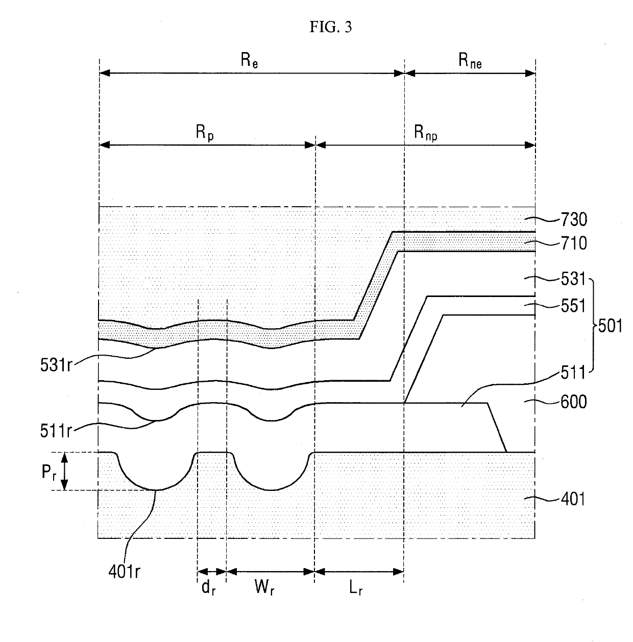
[0217]A driving element layer required for driving the organic light-emitting element was formed on the glass, and an organic layer was formed on the driving element layer to flatten the upper part of the glass. Using a blank mask, a dot-shaped recess pattern having a through-hole in the organic layer was formed at the same time. The depth of the recess pattern was about 0.5 μm and the width was about 2.0 μm. Also, the distance between the recess patterns was about 2.0 μm. Next, the anode electrode was deposited / patterned to form a pixel defining layer, which covers the end portion of the anode electrode. At this time, the minimum horizontal distance between the pixel defining layer and the recess pattern was about 10.0 μm.

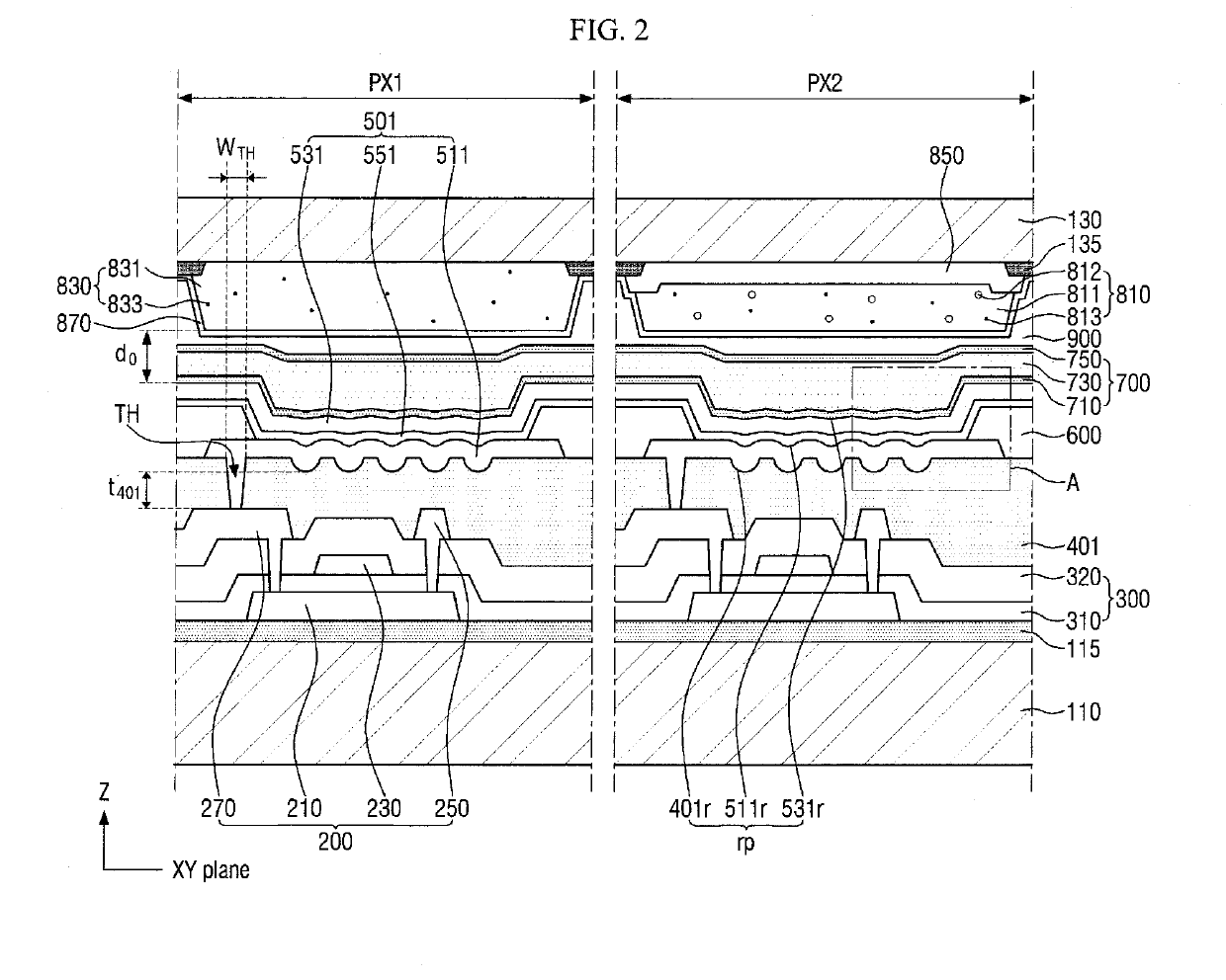
[0218]Subsequently, the organic layer and the cathode electrode were vapor-deposited to form a plurality of organic light-emitting elements that emits blue light in the form as illustrated in FIGS. 2 and 3. In this case, it was possible to check that the recess pa...

experimental example

[0221]The organic light-emitting elements of the test cells manufactured through the Example and the comparative example were driven. The brightness of the light emitted through the blue pixel, the green pixel and the red pixel of the test cells was measured, and illustrated in FIGS. 25 and 26.

[0222]FIG. 25 is a spectrum measurement result of emitted light for each pixel of the test cells according to the Example. FIG. 26 is a spectrum measurement result of emitted light for each pixel of the test cells according to the comparative example. In FIGS. 25 and 26, the luminance of emitted light may be proportional to the lower area of the spectrum.

[0223]First, referring to FIG. 25, it is possible to check that the luminance of the light emitted through the green pixels of the test cell according to the Example is about 13.4% of the luminance of the light emitted through the blue pixel. Assuming that the amount of light emitted by the blue organic light-emitting element is substantially ...


PUM


Abstract

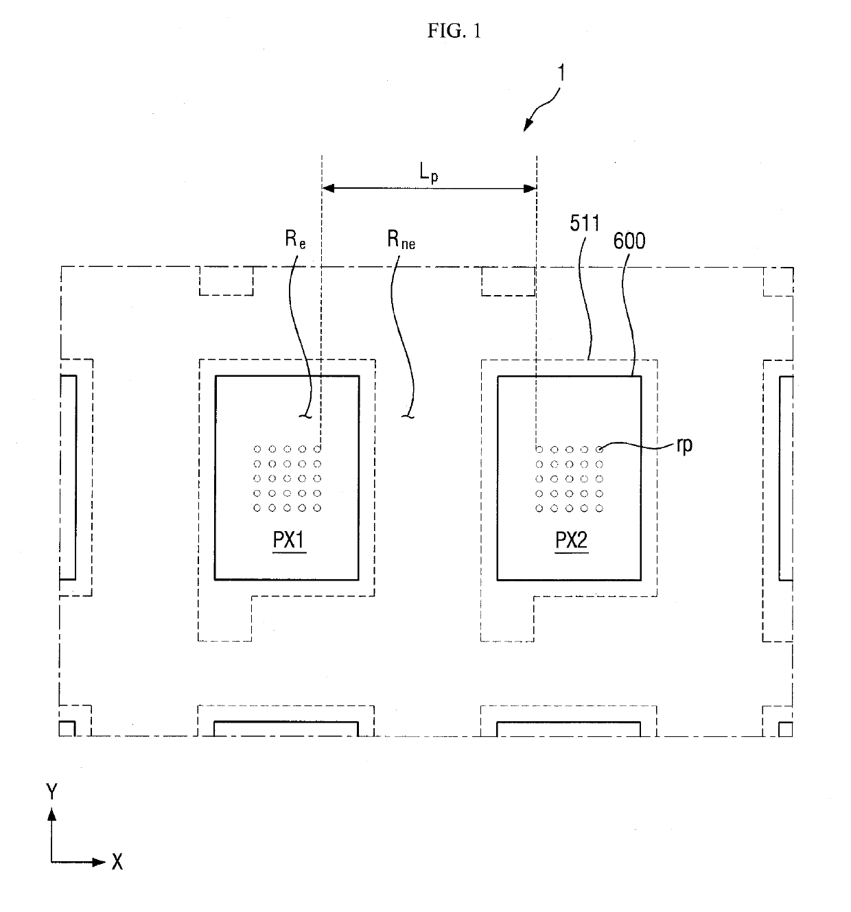
A display device includes a base substrate, an organic layer on the base substrate and including a pattern region having an uneven pattern formed thereon, and a non-pattern region having a substantially flat surface, a light-emitting element on the organic layer, and a color conversion pattern on the light-emitting element and overlapping the pattern region and the non-pattern region.

Description

CROSS-REFERENCE TO RELATED APPLICATION[0001]This application claims priority to Korean Patent Application No. 10-2017-0157901, filed on Nov. 24, 2017, in the Korean Intellectual Property Office, the disclosure of which is incorporated by reference herein in its entirety.BACKGROUND1. Field[0002]Aspects of the present invention relate to a display device and a method of manufacturing a display device.2. Description of the Related Art[0003]A display device, for example, an organic light-emitting display device, includes an organic light-emitting element, which is a self-luminous element. The organic light-emitting element may include two opposing electrodes, and an organic light-emitting layer interposed therebetween. Electrons and holes provided from the two electrodes are recombined in the light-emitting layer to generate excitons, the generated excitons change from an excited state to a ground state, and light may be emitted.[0004]Because such an organic light-emitting display devic...

Claims


Application Information

Patent Timeline
IPC IPC(8): H01L51/52H01L27/32H01L51/56
CPCH01L51/5268H01L27/322H01L27/3246H01L27/3262H01L27/3258H01L51/5209H01L51/5225H01L51/5253H01L27/3248H01L51/56H01L2227/323H01L27/1248H01L2251/558H01L27/3211H10K59/38H10K59/124H10K59/8731H10K59/877H10K59/80515H10K59/35H10K59/1213H10K59/122H10K50/125H10K50/854H10K50/813H10K50/822H10K50/844H10K59/123H10K71/00H10K59/1201H10K2102/351
Inventor CHOI, JUNG HOLEE, JUNE WOO
Owner SAMSUNG DISPLAY CO LTD
Learn More