Plasma display panel

a technology of display panel and plasma, which is applied in the direction of gas discharge vessel/container, gas-filled discharge tube, and electrodes, etc., can solve the problems of increased discharge delay time, increased discharge instability, and increased discharge start voltage and discharge sustain voltage between front substrate electrodes, so as to reduce power consumption and improve discharge stability , the effect of increasing brightness and efficiency

Inactive Publication Date: 2005-05-05
LG ELECTRONICS INC
View PDF2 Cites 8 Cited by
  • Summary
  • Abstract
  • Description
  • Claims
  • Application Information

AI Technical Summary

Benefits of technology

[0020] An object of the present invention to provide a plasma display panel capable of increasing brightness and efficiency without increasing the Xe content.
[0021] Another object of the present invention is to provide a plasma display panel capable of reducing power consumption by lowering a discharge start voltage and a discharge sustain voltage of the PDP.
[0022] Still another object of the present invention is to provide a plasma display panel capable of enhancing discharge stability by shortening a discharge delay time of the PDP.
[0028] According to a plasma display panel of the present invention, brightness and efficiency can be increased without increasing the Xe content. Furthermore, it is possible to reduce power consumption since a discharge start voltage and a discharge sustain voltage are reduced. Discharge stability can be improved since a discharge delay time is shortened.

Problems solved by technology

However, an increase in the Xe content results in a side effect that a discharge start voltage and a discharge sustain voltage between front substrate electrodes are increased.
In addition, as the Xe content increases, the discharge delay time increases.
This results in increased instability of a discharge.
Therefore, it has a problem that the discharge start voltage and the discharge sustain voltage become high.

Method used


Image

  • Plasma display panel
  • Plasma display panel
  • Plasma display panel

Examples


first embodiment

[0059] First Embodiment

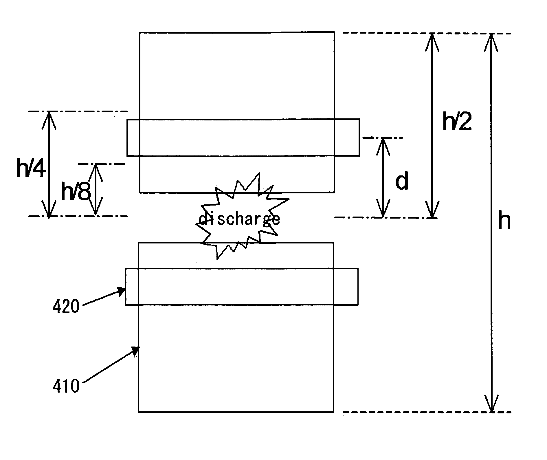
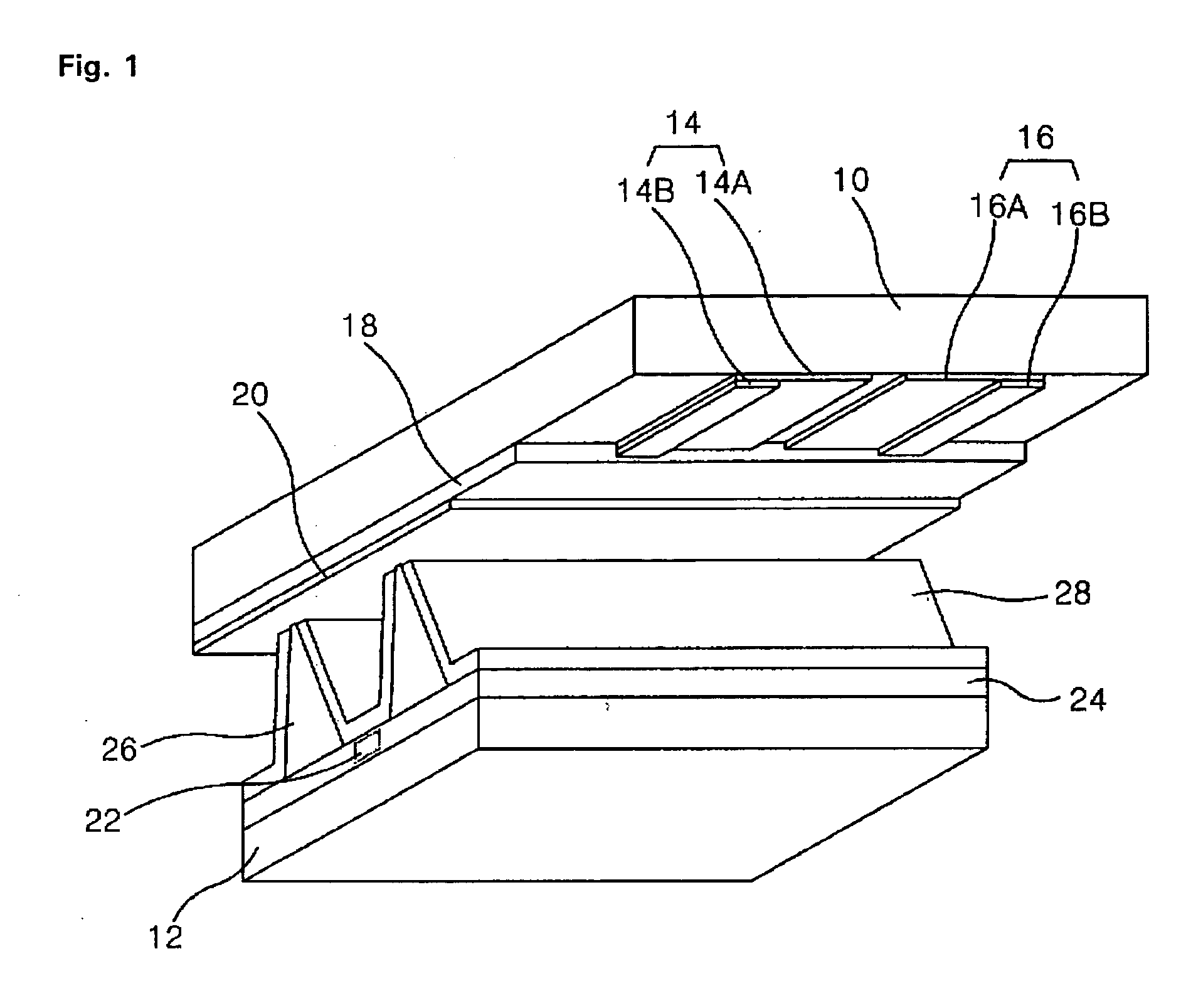
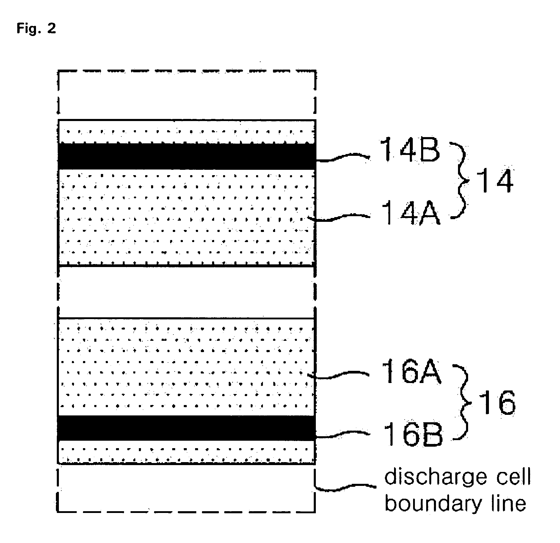
[0060] According to a first embodiment of the present invention, there is provided a plasma display panel having a front substrate and a rear substrate opposite to each other, the plasma display panel including a pair of transparent electrodes formed on the opposite surface of the front substrate, metal electrodes each formed on the transparent electrodes, a dielectric layer that covers the transparent electrodes and the metal electrodes, a protection film coated on the dielectric layer, address electrodes formed on the opposite surface of the rear substrate, a dielectric layer that covers the address electrodes, barrier ribs formed on the dielectric layer, a discharge cell demarcated by the barrier ribs, and a phosphor layer coated on the inside of the discharge cell, wherein assuming that a distance from the center of a discharge region between the pair of the transparent electrodes to the center of the metal electrodes is “d” and a distance between both end...

second embodiment

[0077] Second Embodiment

[0078] According to a second embodiment of the present invention, there is provided a plasma display panel having a front substrate and a rear substrate opposite to each other, the plasma display panel including a pair of transparent electrodes formed on the opposite surface of the front substrate, metal electrodes each formed on the transparent electrodes, a dielectric layer that covers the transparent electrodes and the metal electrodes, a protection film coated on the dielectric layer, address electrodes formed on the opposite surface of the rear substrate, a dielectric layer that covers the address electrodes, barrier ribs formed on the dielectric layer, a discharge cell demarcated by the barrier ribs, and a phosphor layer coated on the inside of the discharge cell, wherein the metal electrodes are formed at locations inclined toward a side where the pair of the transparent electrodes are opposite to each other, and the plasma display panel further compri...

third embodiment

[0105] Third Embodiment

[0106] According to a third embodiment of the present invention, there is provided a plasma display panel having a front substrate and a rear substrate opposite to each other, the plasma display panel including a pair of transparent electrodes formed on the opposite surface of the front substrate, metal electrodes each formed on the transparent electrodes, a dielectric layer that covers the transparent electrodes and the metal electrodes, a protection film coated on the dielectric layer, address electrodes formed on the opposite surface of the rear substrate, a dielectric layer that covers the address electrodes, barrier ribs formed on the dielectric layer, a discharge cell demarcated by the barrier ribs, and a phosphor layer coated on the inside of the discharge cell, wherein the metal electrodes are formed at locations inclined toward a side where the pair of the transparent electrodes are opposite to each other, and the plasma display panel further comprise...


PUM


Abstract

The present invention relates to a plasma display panel, and more particularly, to an electrode structure of a plasma display panel capable of improving brightness and efficiency. According to the present invention, in the plasma display, assuming that a distance from the center of a discharge region between a pair of transparent electrodes to the center of metal electrodes is “d” and a distance between both ends of the pair of the transparent electrodes is “h”, a location on the transparent electrodes of metal electrodes satisfies d<h / 4. Therefore, brightness and efficiency can be increased without increasing the Xe content. Furthermore, it is possible to reduce power consumption since a discharge start voltage and a discharge sustain voltage are lowered. Discharge stability can be improved since a discharge delay time is shortened.

Description

[0001] This Nonprovisional application claims priority under 35 U.S.C. § 119(a) on Patent Application No. 10-2003-0077936 filed in Korea on Nov. 5, 2003, Application No. 10-2004-0032391 filed in Korea on May 7, 2004 and Application No. 10-2004-0042467 filed in Korea on Jun. 10, 2004, the entire contents of which are hereby incorporated by reference. BACKGROUND OF THE INVENTION [0002] 1. Field of the Invention [0003] The present invention relates to a plasma display panel, and more particularly, to an electrode structure of a plasma display panel capable of improving brightness and efficiency. [0004] 2. Description of the Background Art [0005] Various flat panel display devices, which can reduce the weight and volume as shortcomings of the cathode ray tube, have recently been developed. These flat panel display devices include a liquid crystal display (LCD), a field emission display (FED), a plasma display panel (hereinafter, referred to as “PDP”), an electro-luminescence (EL) displa...

Claims


Application Information

Patent Timeline
Patent Type & Authority Applications(United States)
IPC IPC(8): H01J11/12H01J11/14H01J11/22H01J11/24H01J11/26H01J11/34H01J11/36H01J11/38H01J11/40H01J11/42H01J11/50
CPCH01J11/12H01J11/24H01J2211/323H01J11/32H01J2211/245H01J11/28
Inventor MIN, WOONG KEEKANG, JUNG WONPARK, JAE BUM
Owner LG ELECTRONICS INC
Why Eureka
Try Eureka