Liquid crystal display device and method of driving the same

a liquid crystal display and display device technology, applied in the field of liquid crystal display, can solve the problems of increased fabrication low picture quality and increased cost of liquid crystal display device fabrication

Active Publication Date: 2008-05-08
LG DISPLAY CO LTD
View PDF5 Cites 34 Cited by
  • Summary
  • Abstract
  • Description
  • Claims
  • Application Information

AI Technical Summary

Benefits of technology

[0016]A liquid crystal display device comprises a liquid crystal panel including a plurality of data lines formed along a long-axis direction of substrate, and a plurality of gate lines formed along a short-axis direction of substrate. Each gate line is orthogonal to each data l

Problems solved by technology

Also, since the unit cost of source drive integrated circuits ICs 51 and 61 is higher than the unit cost of gate drive integrated circuits ICs 55 and 65, it increases the cost of fabrication of the liquid crystal display device.
Also, the fabrication cost of liquid crystal display device is further increased due to the relatively large size of

Method used


Image

  • Liquid crystal display device and method of driving the same
  • Liquid crystal display device and method of driving the same
  • Liquid crystal display device and method of driving the same

Examples


first embodiment

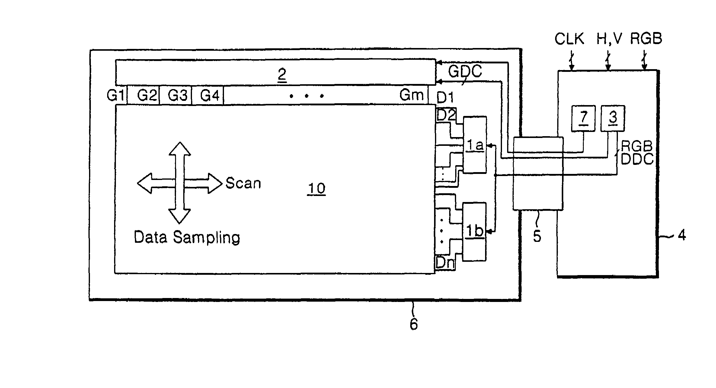
[0056]FIG. 9 is a diagram of illustrating pixel array shown in FIG. 8. Referring to FIG. 9, the pixel array 10 includes the data lines D1 to Dn arranged along the long-axis direction (x) of the liquid crystal panel 6 on the TFT array substrate, and the gate lines G1 to Gm arranged along the short-axis direction (y) of the liquid crystal panel 6 on the TFT array substrate. On the color filter array substrate of the pixel array 10, red, green and blue color filters are arranged along the short-axis direction (y) of the liquid crystal panel 6. Thus, the red, green and blue sub-pixels of the pixel array 10 are arranged along the short-axis direction (y) of the liquid crystal panel 6.

[0057]FIG. 10 is a waveform diagram of illustrating a scan pulse and a data voltage to drive a pixel array of FIG. 9. Referring to FIG. 10, the gate driving circuit 2 sequentially generates the scan pulses which are smaller than one horizontal period (1H), and supplies the generated scan pulses to the gate l...

second embodiment

[0064]FIG. 13 is a diagram of illustrating pixel array shown in FIG. 8. Referring to FIG. 13, the pixel array 10 includes the data lines D1 to Dn arranged along the long-axis direction (x) of the liquid crystal panel 6 on the TFT array substrate, and the gate lines G1 to Gm arranged along the short-axis direction (y) of the liquid crystal panel 6 on the TFT array substrate. On the color filter array substrate of the pixel array 10, red, green and blue color filters are arranged along the long-axis direction (x) of the liquid crystal panel 6. Thus, the red, green and blue sub-pixels of the pixel array 10 are arranged along the long-axis direction (x) of the liquid crystal panel 6.

[0065]FIG. 14 is a waveform diagram of illustrating a scan pulse and a data voltage to drive the pixel array of FIG. 13. As shown in FIG. 14, the gate driving circuit 2 sequentially generates the scan pulse, each of which has a pulse width of about one horizontal period (1H), and supplies the scan pulses to ...

third embodiment

[0071]On the color filter array substrate of the pixel array 10 according to the present disclosure, red, green and blue color filters are arranged along the short-axis direction (y) of the liquid crystal panel 6. Thus, the red, green and blue color sub-pixels of the pixel array 10 are arranged along the short-axis direction (y) of the liquid crystal panel 6. When the two sub-pixels being adjacent to each other use one gate line in common, the sub-pixels R11 to Rn1, B11 to Bn1, G12 to Gn2, R13 to Rn3, . . . G1m to Gnm positioned at the left side of the gate lines G1 to G(3m / 2) are supplied with data from the odd numbered data lines D1, D3, . . . D(2n−1). When the two sub-pixels being adjacent to each other use one gate line in common, the sub-pixels G11 to Gn1, R12 to Rn2, B12 to Bn2, G13 to Gn3 . . . B1m to Bnm positioned at the right side of the gate lines G1 to G(3m / 2) are supplied with data from the even numbered data lines D2, D4, . . . D2n.

[0072]For this, when the thin film t...


PUM


Abstract

A liquid crystal display device and a method of driving the same is disclosed, which can decrease the number of source drive integrated circuits ICs used to supply data, and can also decrease a flexible printed circuit and a printed circuit board to supply signals to the source drive integrated circuits ICs in size. The liquid crystal display device comprises a liquid crystal panel including a plurality of data lines formed along a long-axis direction of substrate, and a plurality of gate lines formed along a short-axis direction of substrate, wherein each gate line is orthogonal to each data line; a data driving circuit to supply data voltages to the data lines; a gate driving circuit to supply scan pulses to the gate lines; and a timing controller to supply digital video data to the data driving circuit, and to control the data driving circuit and the gate driving circuit

Description

CLAIM FOR PRIORITY[0001]This application claims the benefit of Korean Patent Application both Nos. P06-108844 filed on Nov. 6, 2007 and P2007-19574, filed on Feb. 27, 2007, which is hereby incorporated by reference as if fully set forth herein.BACKGROUND[0002]1. Field of the Invention[0003]The present invention relates to a liquid crystal display device which can decrease the number of source drive integrated circuits ICs used to supply data, and also can decrease a flexible printed circuit and a printed circuit board to supply signals to the source drive integrated circuits ICs in size, and a method of driving the same.[0004]2. Description of the Related Art[0005]A liquid crystal display device displays picture images by controlling light transmittance of liquid crystal cells according to video signals. Particularly, an active matrix type liquid crystal display device is suitable for displaying moving pictures since it is provided with switching devices formed in the liquid crystal...

Claims


Application Information

Patent Timeline
IPC IPC(8): G09G5/00G09G3/36
CPCG09G3/3607G09G2320/0209G09G2300/0426G09G3/3648
Inventor KIM, BINNCHO, HYUNG NYUCKKIM, JU PYOUNGCHUN, MIN DOOKWON, OH JONG
Owner LG DISPLAY CO LTD
Why Eureka
Try Eureka