Multi-junction solar cells and methods and apparatuses for forming the same
a solar cell and multi-junction technology, applied in the field of solar cells, can solve the problems of low efficiency, high cost, and high cost of thin film solar cells
- Summary
- Abstract
- Description
- Claims
- Application Information
AI Technical Summary
Problems solved by technology
Method used
Image
Examples
examples
[0045]The examples disclosed herein are exemplary in nature and are not meant to limit the scope of the invention unless explicitly set forth in the claims.
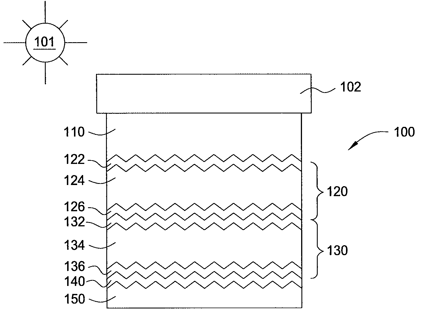
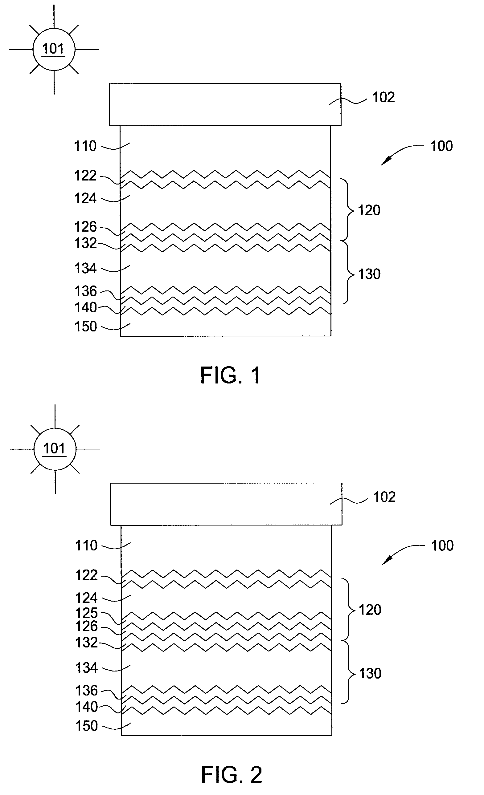
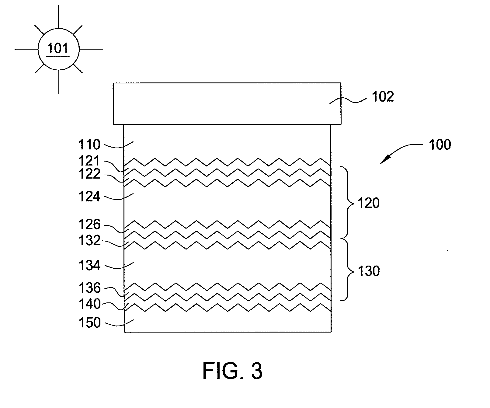
[0046]Substrates having a surface area of 4,320 cm2 were processed in an AKT 4300 PECVD System, available from AKT America, Inc., of Santa Clara, Calif., having an interior chamber volume of 130 liters. Layer 1 was deposited in a first chamber of the PECVD system. Layers 2-4 were deposited in a second chamber of the PECVD system. Layer 5 was deposited in a third chamber of the PECVD system. Layers 6-11 were deposited in a fourth chamber of the PECVD system. The spacing during deposition of layers 1-11 was set to 550 mil and the temperature of the substrate support was set to 200° C. The deposition parameters are set forth in the FIG. 6 to form a tandem p-i-n junction solar cell. Phosphine was provided in a 0.5% mixture in a hydrogen carrier gas. Trimethylborate was provided in a 0.5% mixture in a hydrogen carrier gas. The hydroge...
PUM
 Abstract
Description
Claims
Application Information


