Dynamic pad size to reduce solder fatigue

a pad size and pad technology, applied in the direction of sustainable manufacturing/processing, instruments, final product manufacturing, etc., can solve the problems of mechanical and/or electrical failure of the joint and/or the device, complicating the manufacturing process,

Active Publication Date: 2008-08-07
NXP USA INC
View PDF8 Cites 49 Cited by
  • Summary
  • Abstract
  • Description
  • Claims
  • Application Information

AI Technical Summary

Problems solved by technology

Over time, these forces can cause the solder joint to crack, which may result in mechanical and / or electrical failure of the joint and / or the device.
Most of these approaches are undesirable, however, in that they significantly complicate the manufacturing process.

Method used


Image

  • Dynamic pad size to reduce solder fatigue
  • Dynamic pad size to reduce solder fatigue
  • Dynamic pad size to reduce solder fatigue

Examples


Embodiment Construction

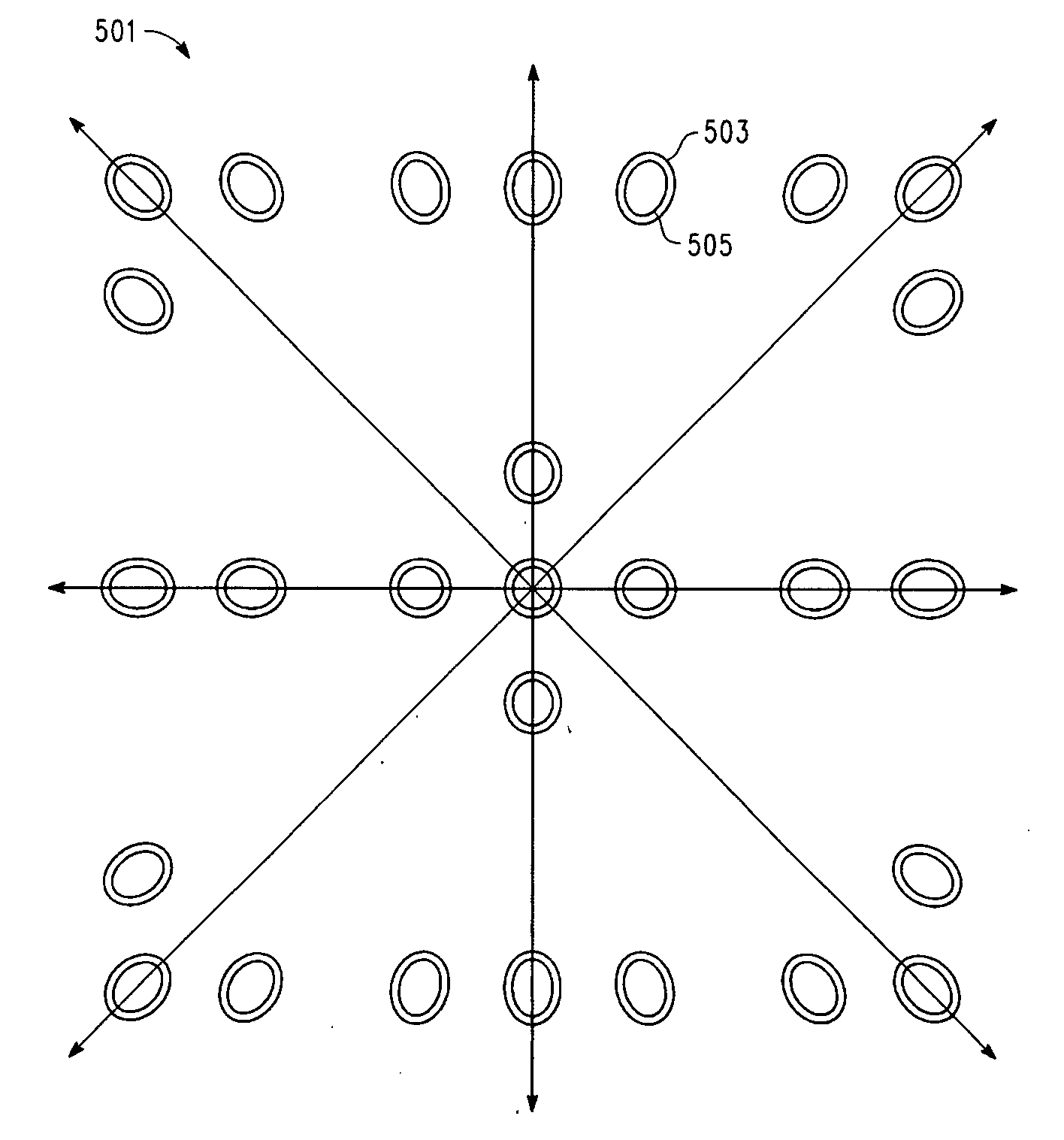
[0017]In one aspect, a method for making a semiconductor device is provided. In accordance with the method, a substrate is provided, and a plurality of bond pads are defined on the substrate. Each bond pad has a major axis and a minor axis in a direction parallel to the substrate, and the ratio of the major axis to the minor axis increases with the distance of a bond pad from the center of the substrate.

[0018]In another aspect, a semiconductor device is provided which comprises a substrate having a plurality of bond pads disposed thereon. Each bond pad has a major axis and a minor axis in a direction parallel to the substrate, and the ratio of the major axis to the minor axis increases with the distance of a bond pad from the center of the substrate.

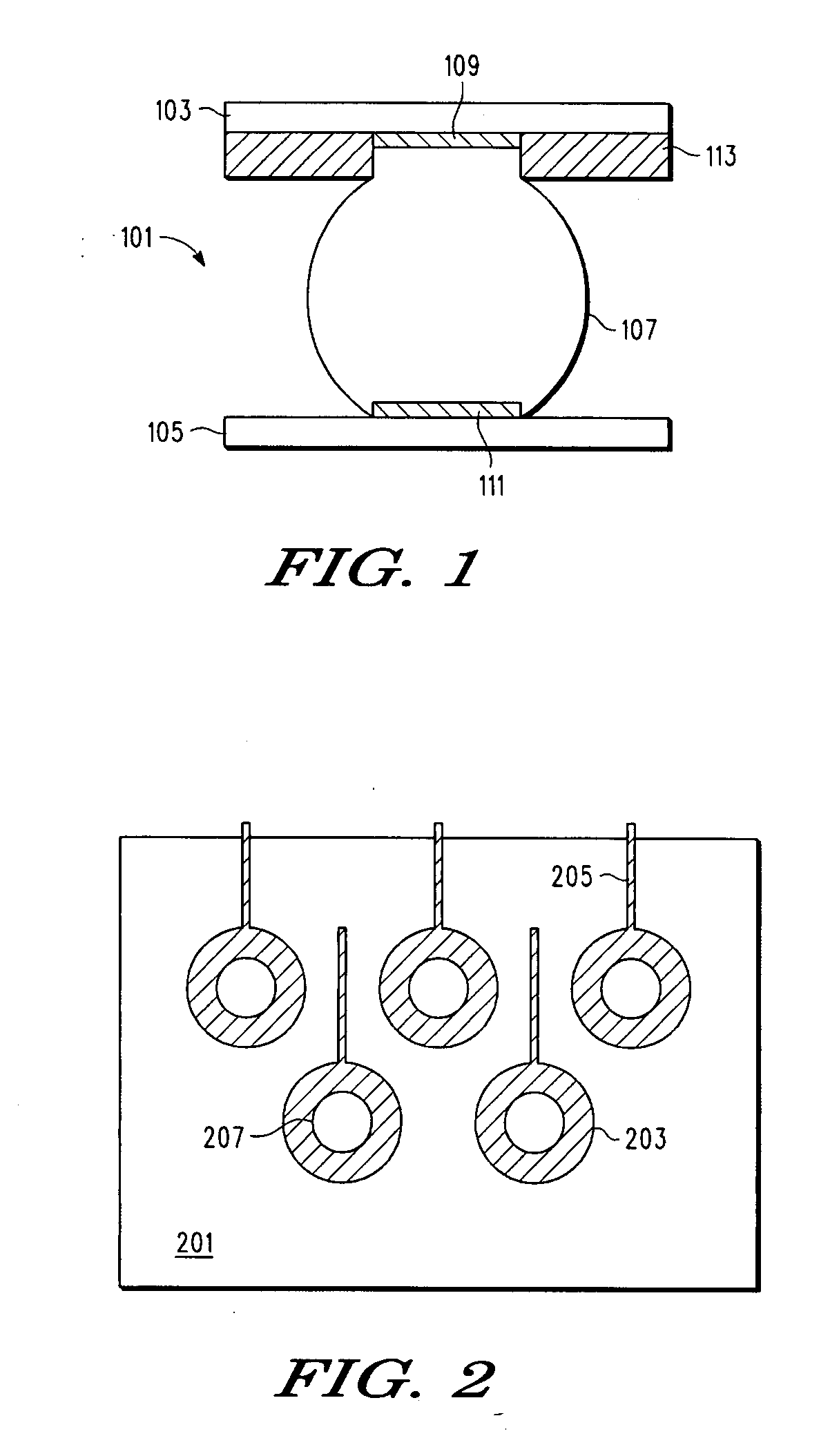
[0019]FIG. 2 illustrates the routing common in a BGA substrate which utilizes solder joints of the type depicted in FIG. 1. As seen therein, the BGA substrate 201 comprises a series of bond pads 203 which are in electrical contact with t...


PUM


Abstract

A semiconductor device is provided which comprises a substrate (501) having a plurality of bond pads (503) disposed thereon. Each bond pad has a major axis and a minor axis in a direction parallel to the substrate, and the ratio of the major axis to the minor axis increases with the distance of a bond pad from the center of the substrate.

Description

FIELD OF THE DISCLOSURE[0001]The present invention relates generally to solder joints, and more particularly to bond pad designs which can be used to improve the integrity of solder joints.BACKGROUND OF THE DISCLOSURE[0002]Solder joints are used widely throughout the semiconductor arts as a convenient means for forming physical and / or electrical connections between device components. Such components may be, for example, a die and an IC packaging substrate, or an IC packaging substrate and a Printed Circuit Board (PCB). Typically, solder joint formation involves the mechanical or electrochemical deposition of solder onto a bond pad which is disposed on a surface of at least one of the components to be joined together, followed by solder reflow.[0003]FIG. 1 illustrates a typical solder joint 101 formed between a Ball Grid Array (BGA) substrate 103 and a die 105. Such a joint, which is common in flip chip packaging, comprises a portion of solder 107 that spans between a first bond pad ...

Claims


Application Information

Patent Timeline
Patent Type & Authority Applications(United States)
IPC IPC(8): H01L23/485G06F17/50H01L21/60
CPCH01L23/49838H01L24/16H01L2224/16H05K2201/10734H05K3/3436H05K2201/09418H05K1/111H01L2224/0401H01L2224/0554H01L2224/05568H01L2224/05573H01L2224/141H01L2924/00014Y02P70/50H01L2224/05599H01L2224/0555H01L2224/0556H05K3/34
Inventor PHAM, TIM V.UEHLING, TRENT S.
Owner NXP USA INC
Why Eureka
Try Eureka