
Method for reducing dielectric overetch using a dielectric etch stop at a planar surface

a dielectric etch stop and planar surface technology, applied in the direction of diodes, semiconductor devices, electrical apparatus, etc., can solve the problems of excessive dielectric overetch, design and device may have particularly limited tolerance for dielectric overetch, etc., to prevent excessive dielectric overetch

Inactive Publication Date: 2008-10-16
SANDISK TECH LLC
View PDF39 Cites 15 Cited by
  • Summary
  • Abstract
  • Description
  • Claims
  • Application Information

AI Technical Summary

Benefits of technology

[0006]The present invention is defined by the following claims, and nothing in this section should be taken as a limitation on those claims. In general, the invention is directed to a method to prevent excessive dielectric overetch when making electrical contact to conductive or semiconductor features.
[0007]A first aspect of the invention provides for a method for reducing dielectric overetch, the method comprising: forming a substantially planar surface, wherein the planar surface coexposes conductive or semiconductor features and a dielectric etch stop layer; depositing second dielectric fill directly on the planar surface; and etching a void in the second dielectric fill, wherein the etch is selective between the second dielectric fill and the dielectric etch stop layer, wherein the etch stops on the dielectric etch stop layer.
[0010]Another preferred embodiment of the invention provides for a method for minimizing dielectric overetch in a monolithic three dimensional memory array, the method comprising: forming a first memory level by a method comprising: forming first bottom conductors; forming first pillars above the first bottom conductors, the first pillars separated by a first dielectric material; depositing a second dielectric material on the first pillars; etching trenches in the second dielectric material, wherein the etch is selective between the first dielectric material and the second dielectric material; and forming first top conductors in the trenches; and monolithically forming at least a second memory level above the first memory level.

Problems solved by technology

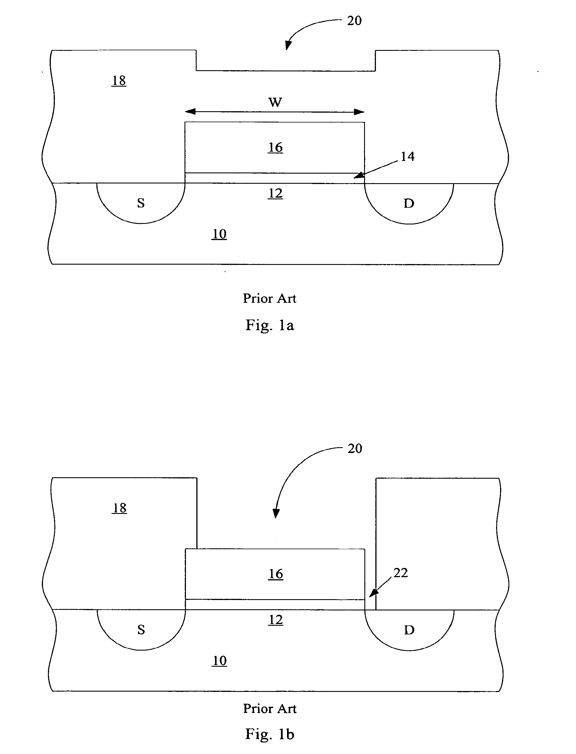
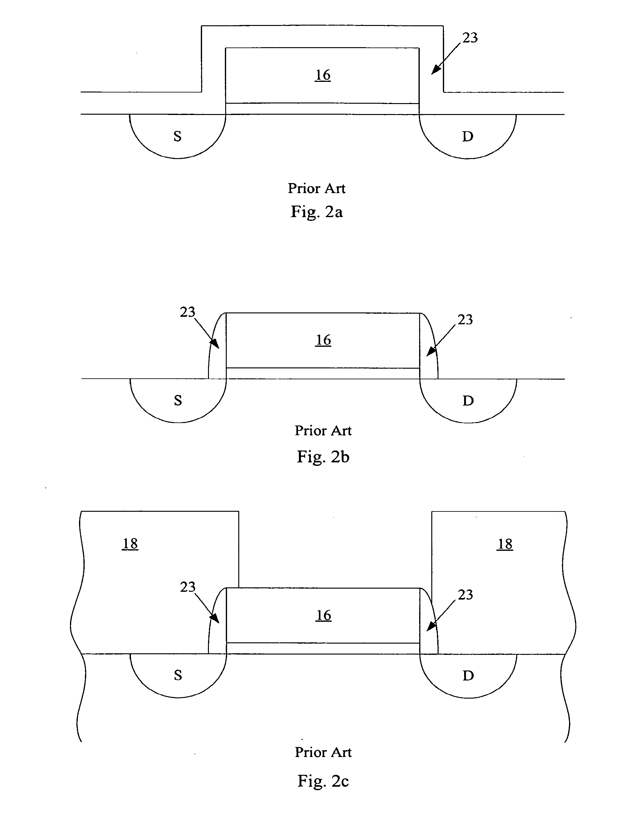
If the etch is misaligned, some portion of the etched region may not fall on the conductive or semiconductor feature, instead continuing into fill dielectric, and excessive overetch may occur in this misaligned region.
Some designs and devices may have particularly limited tolerance for dielectric overetch.

Method used


Image

  • Method for reducing dielectric overetch using a dielectric etch stop at a planar surface
  • Method for reducing dielectric overetch using a dielectric etch stop at a planar surface
  • Method for reducing dielectric overetch using a dielectric etch stop at a planar surface

Examples


example

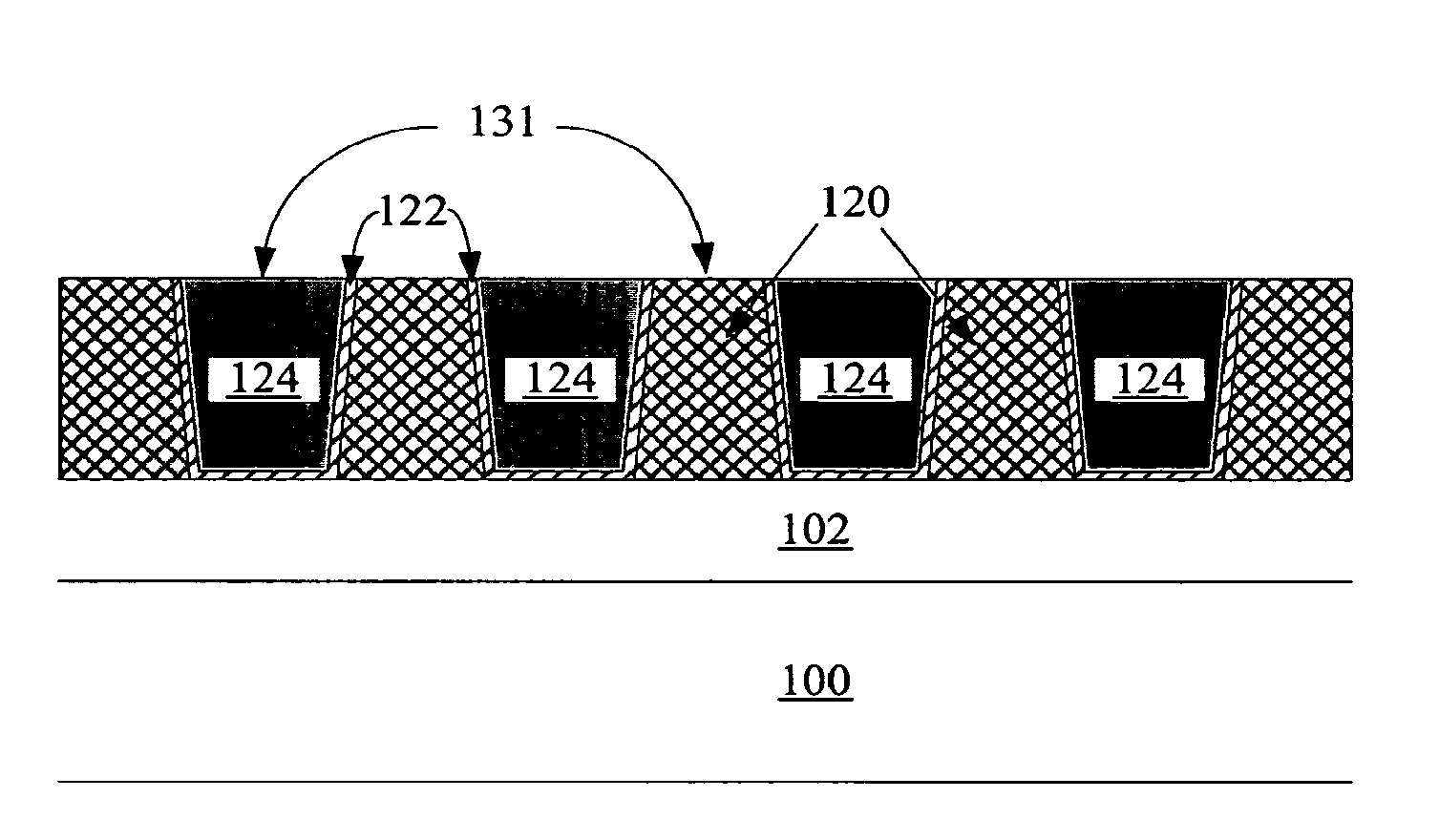
[0053]Fabrication of a single memory level is described. Additional memory levels can be stacked, each monolithically formed above the one below it.

[0054]Turning to FIG. 9a, formation of the memory begins with a substrate 100. This substrate 100 can be any semiconducting substrate as known in the art, such as monocrystalline silicon, IV-IV alloys like silicon-germanium or silicon-germanium-carbon, III-V alloys, II-VII alloys, epitaxial layers over such substrates, or any other semiconducting material. The substrate may include integrated circuits fabricated therein.

[0055]An insulating layer 102 is formed over substrate 100. The insulating layer 102 can be silicon oxide, silicon nitride, high-dielectric film, Si—C—O—H film, or any other suitable insulating material. In this example, insulating layer 102 is silicon dioxide, and this layer is, for example, about 3500 angstroms thick.

[0056]The first conductors 200 are formed over insulating layer 102. An adhesion layer 104 may be includ...


PUM


Abstract

A substantially planar surface coexposes conductive or semiconductor features and a dielectric etch stop material. A second dielectric material, different from the dielectric etch stop material, is deposited on the substantially planar surface. A selective etch etches a hole or trench in the second dielectric material, so that the etch stops on the conductive or semiconductor feature and the dielectric etch stop material. In a preferred embodiment the substantially planar surface is formed by filling gaps between the conductive or semiconductor features with a first dielectric such as oxide, recessing the oxide, filling with a second dielectric such as nitride, then planarizing to coexpose the nitride and the conductive or semiconductor features.

Description

RELATED APPLICATIONS[0001]This application is related to Petti, “Method for Reducing Dielectric Overetch When Making Contact to Conductive Features,” U.S. application Ser. No. ______, (attorney docket number MA-137), filed on even date herewith and hereby incorporated by reference.BACKGROUND OF THE INVENTION[0002]The invention relates to a method for reducing dielectric overetch when making contact to conductive features, where those conductive features are interspersed with a dielectric material in a substantially planar surface. The method makes use of etch selectivities between different dielectric materials.[0003]In semiconductor devices, it is known to etch through a dielectric material to make electrical contact to a conductive or semiconductor feature which is covered by the dielectric material. Electrical contact may be made by way of a via, for example, or by formation of a conductor formed by a damascene method.[0004]The etch is ideally aligned with the buried conductive o...

Claims


Application Information

Patent Timeline
Patent Type & Authority Applications(United States)
IPC IPC(8): H01L21/306H01L21/768
CPCH01L21/76802H01L21/76829H01L27/1021Y10S438/90H01L21/31H01L21/306H01L21/768H10B99/00
Inventor DUNTON, SAMUEL V.PETTI, CHRISTOPHER J.RAGHURAM, USHA
Owner SANDISK TECH LLC
Learn More