Test circuit

a test circuit and circuit technology, applied in the field of test circuits, can solve problems such as the difficulty of miniaturizing the semiconductor device, the failure of the system to operate normally, and the problem of the technique disclosed

Inactive Publication Date: 2008-11-13
RENESAS ELECTRONICS CORP
View PDF12 Cites 48 Cited by
  • Summary
  • Abstract
  • Description
  • Claims
  • Application Information

AI Technical Summary

Benefits of technology

[0015]According to the test circuit of the present invention, the selecting circuit generates internal TMS signal based on TMS signal input from the TMS terminal provided for each of the plurality of TAP controllers and controls the output destination of the internal TMS signal. Further, the TAP controllers provided in the first and second controllers perform behavior complied with IEEE1149. Therefore, according to the test circuit of the present invention, each of the plurality of TAP controllers can be operated without violating standard of IEEE1149 by selecting the TAP controller controlling and operating the output destination of the internal TMS signal by the selecting circuit.
[0016]According to the test circuit of the present invention, it is possible to control each of the plurality of TAP controllers using instruction code complied with IEEE1149 and a set of test access ports without violating standard specification of IEEE1149.

Problems solved by technology

A package of the semiconductor device becomes larger and miniaturization of the semiconductor device is difficult as the number of terminals is increased.
However, we have now discovered that there are problems in the techniques disclosed in related art 1 to related art 4.
Therefore, incompatibility of the instruction code may be raised among semiconductor devices when the circuits are implemented on the substrate with other semiconductor devices, which causes malfunction of behavior of the system.
Therefore, incompatibility of the operation procedure may be raised among semiconductor devices when the circuits are implemented on the board with other semiconductor devices, which causes malfunction of behavior of the system.

Method used


Image

  • Test circuit
  • Test circuit
  • Test circuit

Examples


first embodiment

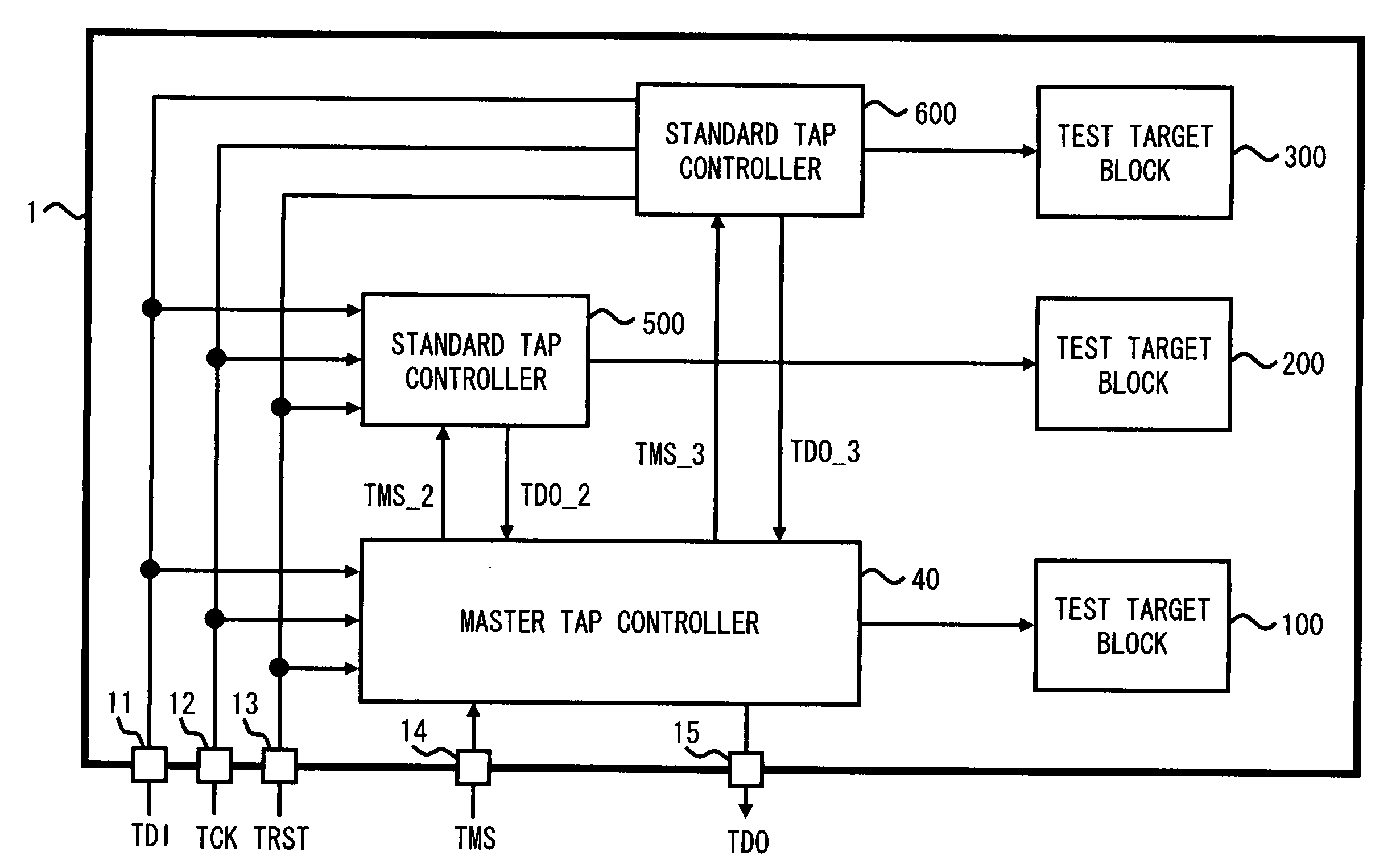
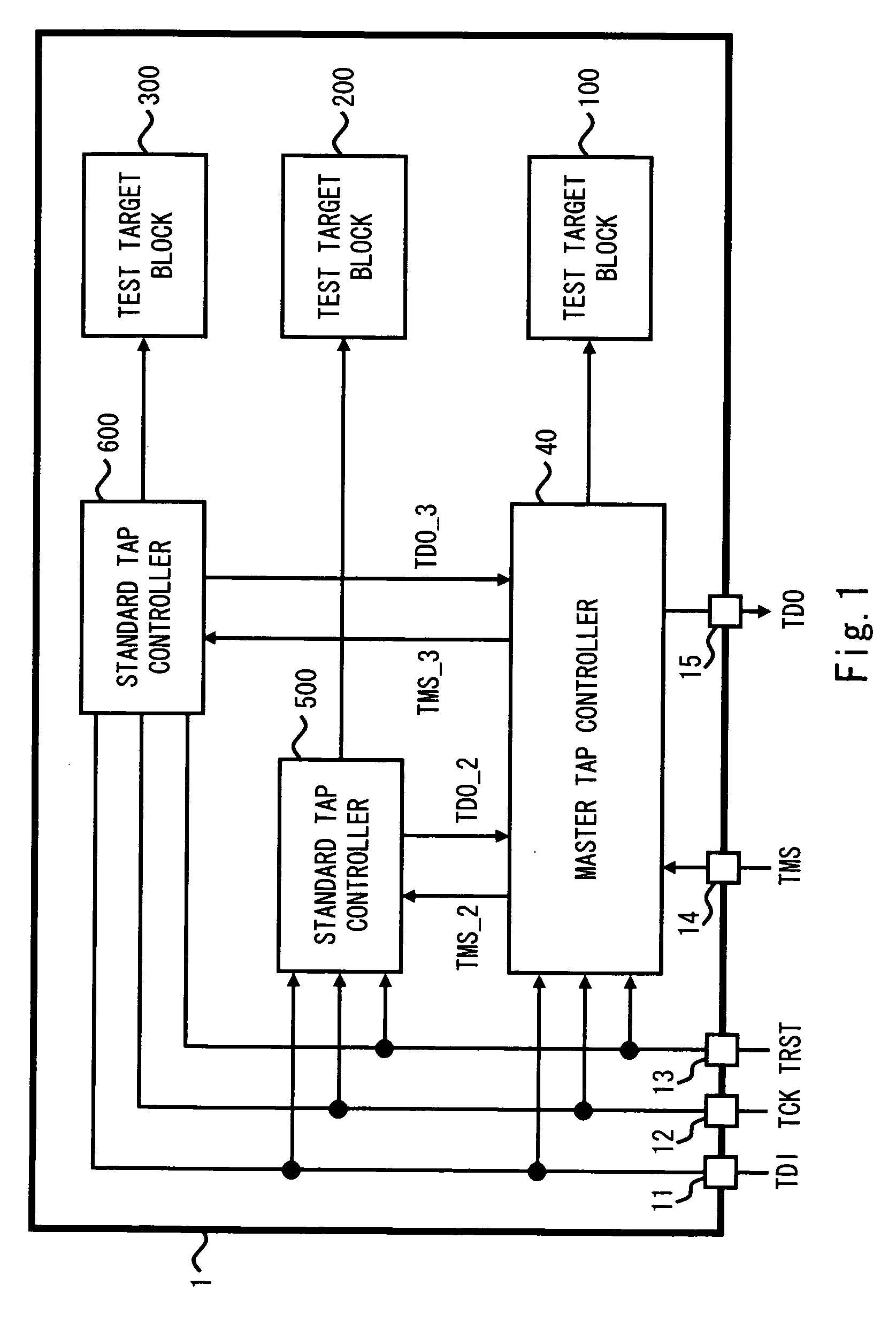
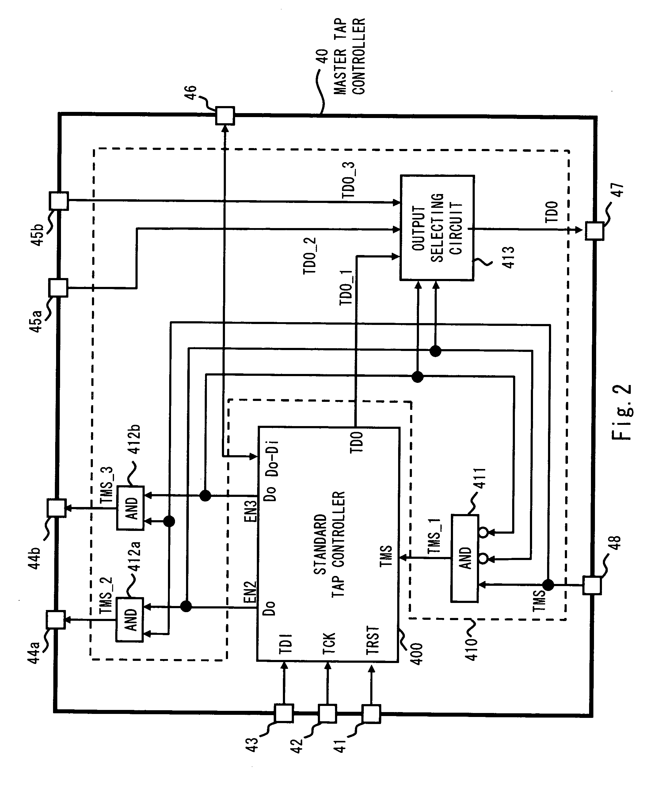
[0044]FIG. 1 shows a block diagram of a semiconductor device 1 according to the present embodiment. As shown in FIG. 1, the semiconductor device 1 includes a TDI terminal 11, a TCK terminal 12, a TRST terminal 13, a TMS terminal 14, a TDO terminal 15, test target blocks 100 to 300, a first controller (master TAP controller, for example) 40, and second controllers (standard TAP controllers, for example) 500, 600. In the following embodiment, circuit part excluding the test target blocks from the semiconductor device 1 is called test circuit. The test circuit includes a first TAP controller having a function of decoding an instruction code for selection and a second TAP controller which does not have to have a function of decoding the instruction code for selection. In the following description, a standard TAP controller 400 embedded in the master TAP controller corresponds to the first TAP controller and the standard TAP controllers 500 and 600 correspond to the second TAP controller...

second embodiment

[0076]FIG. 5 shows a block diagram of a semiconductor device 2 according to the second embodiment. As shown in FIG. 5, the test circuit according to the second embodiment includes a third controller (a sub-master TAP controller, for example) 50 in addition to the master TAP controller 40. The sub-master TAP controller 50 outputs the second internal TMS signal TMS_4 to a standard TAP controller 800 based on the first internal TMS signal TMS_2 output from the master TAP controller and the instruction code for selection. Note that the sub-master TAP controller 50 includes a third TAP controller including a function of decoding the instruction code for selection. In the present embodiment, the standard TAP controller 500 embedded in the sub-master TAP controller 50 corresponds to the third TAP controller.

[0077]FIG. 6 shows a block diagram of the sub-master TAP controller. As shown in FIG. 6, the sub-master controller includes a standard TAP controller 500 and a selecting circuit 510. In...

third embodiment

[0081]FIG. 7 shows a block diagram of a semiconductor device 3 according to the third embodiment. As shown in FIG. 7, in the test circuit according to the third embodiment, the first internal TMS signal TMS_3 is input to the two standard TAP controllers of the standard TAP controllers 600 and 800. In this case, since only up to three output signals TDO can be selected in the master TAP controller 40, arbitration is performed on the output signal TDO_3 and the output signal TDO_4 using an OR gate 900 as an arbitration circuit.

[0082]As stated above, it is possible to input the first internal TMS signal to the plurality of standard TAP controllers by performing arbitration on the output signal TDO by the arbitration circuit.


PUM


Abstract

A test circuit including a TAP controller specified in IEEE (Institute of Electrical and Electronics Engineers) 1149 and a test access port includes a first controller including a selecting circuit and a first TAP controller, the selecting circuit generating an internal TMS signal in accordance with TMS signal and selecting an output destination of the internal TMS signal in accordance with a selection signal, and the first TAP controller changing internal state based on the internal TMS signal, testing corresponding test target block in accordance with instruction code for test, and generating the selection signal in accordance with instruction code for selection, and a second controller including a second TAP controller changing internal state based on the internal TMS signal and testing corresponding test target block in accordance with the instruction code for test.

Description

BACKGROUND OF THE INVENTION[0001]1. Field of the Invention[0002]The present invention relates to a test circuit, and more particularly, to a test circuit including a TAP (Test Access Port) controller defined in IEEE1149.[0003]2. Description of Related Art[0004]A circuit size of a semiconductor device has recently become larger and larger, and a number of terminals performing test on the semiconductor device has been increasing. A package of the semiconductor device becomes larger and miniaturization of the semiconductor device is difficult as the number of terminals is increased. It is therefore required to reduce the number of terminals. In order to achieve this, IEEE (Institute of Electrical and Electronics Engineers) has defined IEEE1149. With IEEE1149.1, which is one of IEEE1149, it is possible to perform test of the semiconductor device using five terminals and a TAP controller. The five terminals are called a TDI terminal, a TRST terminal, a TCK terminal, a TMS terminal, and a...

Claims


Application Information

Patent Timeline
Patent Type & Authority Applications(United States)
IPC IPC(8): G01R31/317
CPCG01R31/31855
Inventor NAKAMURA, YOSHIYUKIASAKA, TOSHIHARUMAEDA, TOSHIYUKISASAKI, TOMONORI
Owner RENESAS ELECTRONICS CORP
Why Eureka
Try Eureka