Integral photography type three-dimensional display device
a display device and photography technology, applied in the field of three-dimensional display devices, can solve the problems of limited depth range given to the displayed imag
- Summary
- Abstract
- Description
- Claims
- Application Information
AI Technical Summary
Benefits of technology
Problems solved by technology
Method used
Image
Examples
first embodiment
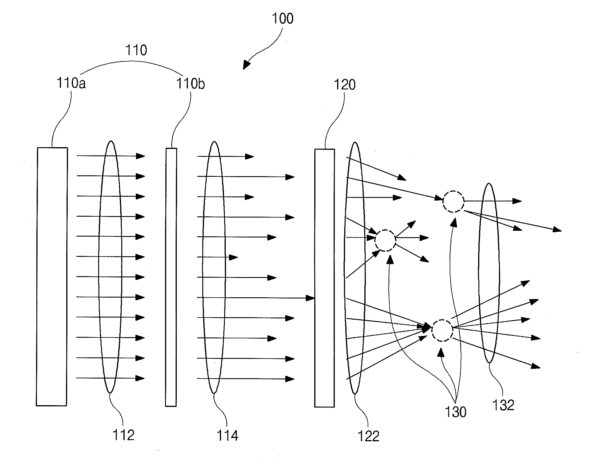
[0036]FIG. 3 is a view illustrating an integral photography type three-dimensional display device according to the disclosure.
[0037]Referring to FIG. 3, the integral photography type display device 100 includes a brightness control panel 110 and a path control panel 120. The brightness control panel 110 may include a backlight unit 110a and a liquid crystal panel 110b including a plurality of pixels in a matrix form.
[0038]The brightness control panel 110 control brightness of a ray passing through each pixel.
[0039]To prevent interference by adjacent pixels, the backlight unit 110a has a high-condensing property so that a plurality of first rays 112 is emitted from the backlight unit 110a within about a 10 degree angle with respect to a perpendicular line to a plane of the liquid crystal panel 120a. Accordingly, the first rays 112 have uniform brightness and are incident on the liquid crystal panel 110b.
[0040]The liquid crystal panel 110b controls transmissivity of each pixel accord...
second embodiment
[0071]FIG. 6A is a perspective view illustrating a path control panel of an integral photography type three-dimensional display device according to the present invention, and FIG. 6B is a cross-sectional view taken along a line VI-VI of FIG. 6A.
[0072]Referring to FIGS. 6A and 6B, the path control panel 220 may have a different structure from the path control panel of FIGS. 5A and 5B. The integral photography type three-dimensional display device of the second embodiment may be similar to that of the first embodiment except for the path control panel.
[0073]The path control panel 220 may include third and fourth substrates 240 and 242 and a second liquid crystal layer 244 between the third and fourth substrates 240 and 242. The path control panel 220 includes first and second path pixels Pb1 and Pb2 corresponding to the first and second brightness pixels (Pa1 and Pa2 of FIG. 4), respectively.
[0074]Each of the first and second path pixels Pb1 and Pb2 includes a first electrode 246 on a...
PUM
 Abstract
Description
Claims
Application Information


