Eureka AIR delivers breakthrough ideas for toughest innovation challenges, trusted by R&D personnel around the world.

Electronic component and method of forming the same

Inactive Publication Date: 2009-01-15
YAMAHA CORP
View PDF6 Cites 2 Cited by
  • Summary
  • Abstract
  • Description
  • Claims
  • Application Information

AI Technical Summary

Benefits of technology

[0013]It is another object of the present invention to provide a connector that allows first and second electronic components to be stacked in a direction vertical to the surface of a substrate, wherein the first electronic component has a first two-dimensional alignment of terminals at narrow pitch, and the second electronic component has a second two-dimensional alignment of terminals at narrow pitch, and wherein the connector connects one of the first two-dimensional alignment of terminals and one of the second two-dimensional alignment of terminals.
[0028]In the first typical case, the external electrode is the projecting electrode having the head portion which is snap-fitted to the hollow portion of the connector. In this case, the at least one sloped guiding surface may be sloped down inwardly, and the at least one stopper projects inwardly. For connecting the electronic component to the counterpart electronic component, the head portion of the projecting electrode is made into contact slidably with the down-sloped guiding surface. Since the base may be elastic and deformable, forcing the head portion of the projecting electrode toward the down-sloped guiding surface may cause that the free end of the base moves outwardly until the head portion of the electrode is snapped into the hollow structure of the connector. The head portion of the projecting electrode is snap-fitted into the connector. The base being elastic may cause that the base fits and holds the head portion of the projecting electrode. The at least one stopper also holds the head portion of the projecting electrode. Since the base is electrically conductive, the connector and the projecting electrode are electrically connected. Using the connector allows that the electronic component and the counterpart electronic component are stacked each other over the substrate and both the components are electrically connected to each other. The elasticity and deformability of the base of the connector allows that the head portion of the projecting electrode is snap-fitted into the connector. Thus, a two-dimensional dense array at narrower pitch of the connectors over the substrate can be obtainable.
[0030]In the second typical case, the external electrode is the electrode having the through hole which is snap-fitted to the connector. In this case, the at least one sloped guiding surface may be sloped down outwardly, and the at least one stopper projects outwardly. For connecting the electronic component to the counterpart electronic component, the electrode having the through hole is made into contact slidably with the down-sloped guiding surface. Since the base may be elastic and deformable, forcing the electrode toward the down-sloped guiding surface may cause that the free end of the base moves inwardly until the electrode with the through hole is snapped into the connector. The electrode with the through hole is snap-fitted into the connector. The base being elastic may cause that the base fits and holds the electrode. The at least one stopper also holds the electrode. Since the base is electrically conductive, the connector and the electrode are electrically connected. Using the connector allows that the electronic component and the counterpart electronic component are stacked each other over the substrate and both the components are electrically connected to each other. The elasticity and deformability of the base of the connector allows that the electrode is snap-fitted into the connector. Thus, a two-dimensional dense array at narrower pitch of the connectors over the substrate can be obtainable.
[0037]The external electrode is the projecting electrode having the head portion which is snap-fitted to the hollow portion of the connector. In this case, the at least one sloped guiding surface may be sloped down inwardly, and the at least one stopper projects inwardly. For connecting the electronic component to the counterpart electronic component, the head portion of the projecting electrode is made into contact slidably with the down-sloped guiding surface. Since the base may be elastic and deformable, forcing the head portion of the projecting electrode toward the down-sloped guiding surface may cause that the free end of the base moves outwardly until the head portion of the electrode is snapped into the hollow structure of the connector. The head portion of the projecting electrode is snap-fitted into the connector. The base being elastic may cause that the base fits and holds the head portion of the projecting electrode. The at least one stopper also holds the head portion of the projecting electrode. Since the base is electrically conductive, the connector and the projecting electrode are electrically connected. Using the connector allows that the electronic component and the counterpart electronic component are stacked each other over the substrate and both the components are electrically connected to each other. The elasticity and deformability of the base of the connector allows that the head portion of the projecting electrode is snap-fitted into the connector. Thus, a two-dimensional dense array at narrower pitch of the connectors over the substrate can be obtainable.
[0045]The external electrode is the electrode having the through hole which is snap-fitted to the connector. In this case, the at least one sloped guiding surface may be sloped down outwardly, and the at least one stopper projects outwardly. For connecting the electronic component to the counterpart electronic component, the electrode having the through hole is made into contact slidably with the down-sloped guiding surface. Since the base may be elastic and deformable, forcing the electrode toward the down-sloped guiding surface may cause that the free end of the base moves inwardly until the electrode with the through hole is snapped into the connector. The electrode with the through hole is snap-fitted into the connector. The base being elastic may cause that the base fits and holds the electrode. The at least one stopper also holds the electrode. Since the base is electrically conductive, the connector and the electrode are electrically connected. Using the connector allows that the electronic component and the counterpart electronic component are stacked each other over the substrate and both the components are electrically connected to each other. The elasticity and deformability of the base of the connector allows that the electrode is snap-fitted into the connector. Thus, a two-dimensional dense array at narrower pitch of the connectors over the substrate can be obtainable.

Problems solved by technology

Shrinkage of the microconnectors is not easy due to placing a magnet.
Shrinkage of the microconnectors is not easy.
The microconnectors have poor mechanical durability.

Method used


Image

  • Electronic component and method of forming the same
  • Electronic component and method of forming the same
  • Electronic component and method of forming the same

Examples


first embodiment

Configurations of Electronic Components:

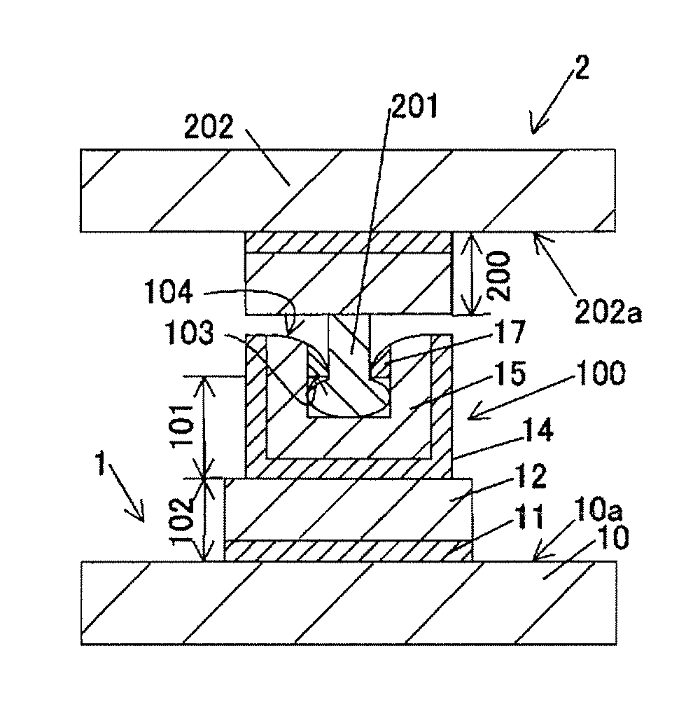
[0089]FIG. 1A is a cross sectional elevation view illustrating a first electronic component 1 and a second electronic component 2 that is connected to the first electronic component1 in accordance with a first preferred embodiment of the present invention. FIG. 1B is a plan view illustrating the first electronic component shown in FIG. 1A which is a view taken along a 1A-1A line of FIG. 1B.

First Electronic Component 1:

[0090]A first electronic component 1 can be configured to be connected to a second electronic component 2. In some cases, the first electronic component 1 may include, but is not limited to, a substrate 10, and a connector 100. The substrate 10 may have a bonding surface 10a that has a conductive interconnection element thereon such as a surface interconnection 102. In some cases, the surface interconnection 102 may include, but is not limited to, a multilayered structure of a seed layer 11 and a conductive film 12.

[0091]The conn...

second embodiment

Configurations of Electronic Components:

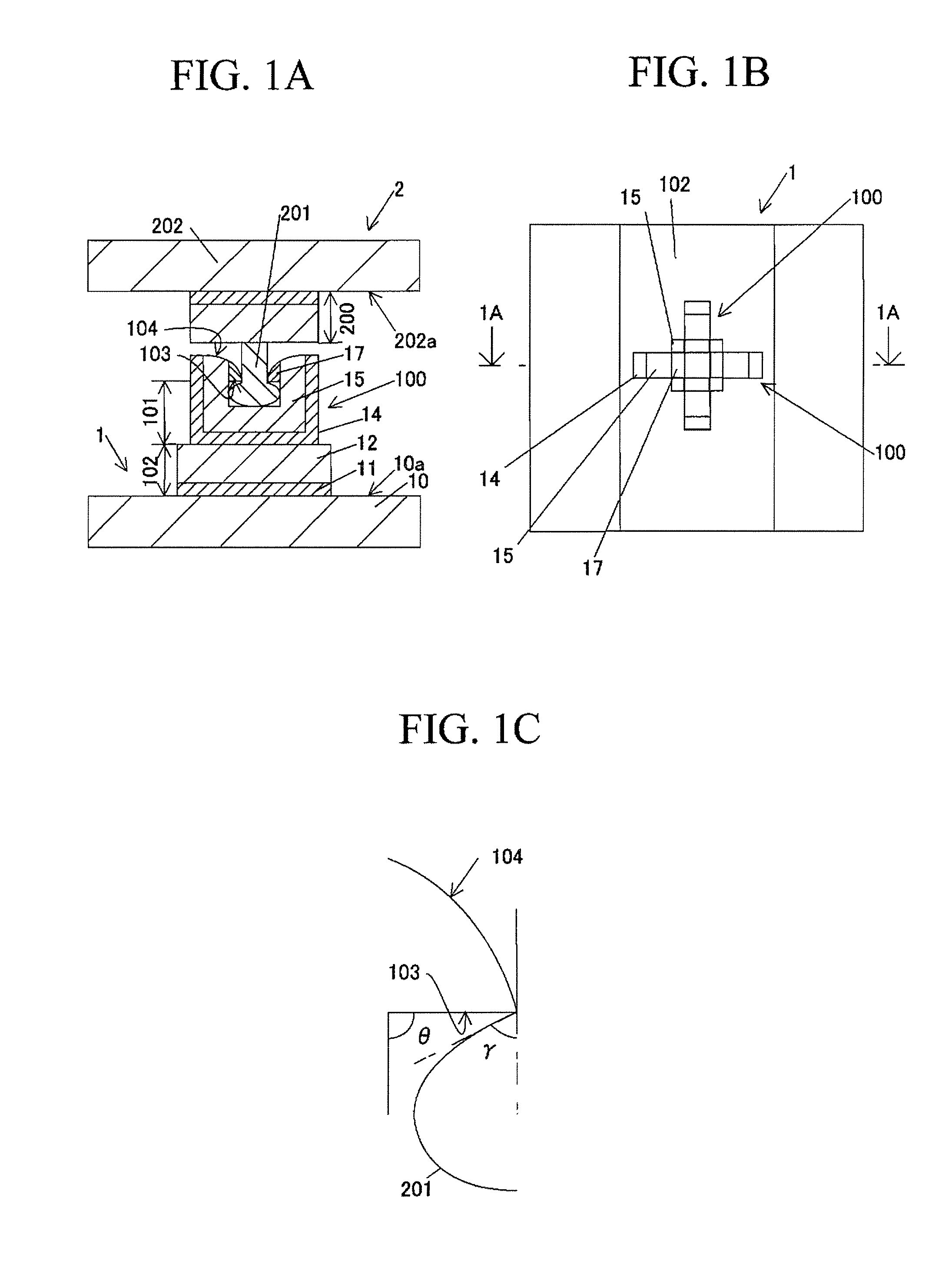
[0106]FIG. 2A is a cross sectional elevation view illustrating a third electronic component 3 and the second electronic component 2 that is connected to the third electronic component 3 in accordance with a second preferred embodiment of the present invention. FIG. 2B is a plan view illustrating the third electronic component shown in FIG. 2A which is a view taken along a 2A-2A line of FIG. 2B.

[0107]The second electronic component 2 of this embodiment is the same as the second electronic component 2 of the first embodiment. The third electronic component 3 of this embodiment is different from the first electronic component 1 of the first embodiment. The third electronic component 3 may have guiding surfaces 105 which are sloped down toward the center of the connector 100. In some cases, the guiding surfaces 105 may be sloped planes and non-curved surfaces. In particular cases, the sloped planes may have an angle of about 45 degrees. The downwa...

third embodiment

[0108]Configurations of Electronic Components:

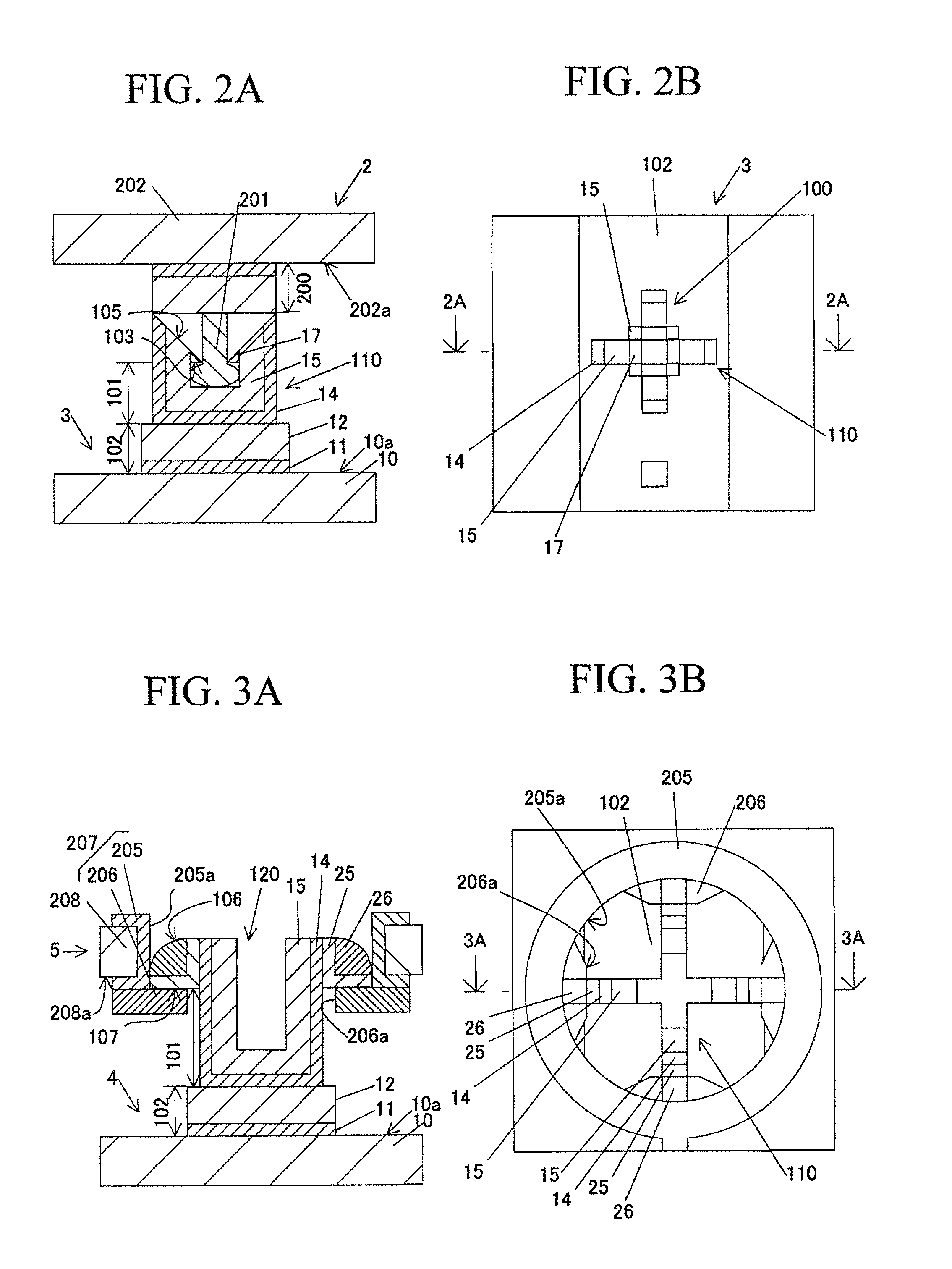
[0109]FIG. 3A is a cross sectional elevation view illustrating a fourth electronic component 4 and a fifth electronic component 5 that is connected to the fourth electronic component 4 in accordance with a third preferred embodiment of the present invention. FIG. 3B is a plan view illustrating the third electronic component shown in FIG. 3A which is a view taken along a 3A-3A line of FIG. 3B.

Fourth Electronic Component 4:

[0110]A fourth electronic component 4 can be configured to be connected to a fifth electronic component 5. In some cases, the fourth electronic component 4 may include, but is not limited to, a substrate 10, and a connector 120. The substrate 10 may have a bonding surface 10a that has a conductive interconnection element thereon such as a surface interconnection 102. In some cases, the surface interconnection 102 may include, but is not limited to, a multilayered structure of a seed layer 11 and a conductive film 12.

[011...


PUM

PropertyMeasurementUnit
Electrical conductivityaaaaaaaaaa
Electrical conductoraaaaaaaaaa
Elasticityaaaaaaaaaa

Abstract

An electronic component includes a substrate, an interconnection element, and a connector. The interconnection element has conductivity. The interconnection element is present over the substrate. The connector is present on the interconnection element. The connector may further include, but is not limited to, a base, at least one stopper, and at least one sloped guiding surface. The base projects from the interconnection element in a first direction that is vertical to the surface of the substrate. At least one stopper projects from the base in a second direction that is parallel to the surface of the substrate. The one stopper has a stopper surface.

Description

BACKGROUND OF THE INVENTION[0001]1. Field of the Invention[0002]The present invention generally relates to an electronic component and a method of forming the same. More specifically, the present invention relates to a microconnector and a method of forming the same.[0003]Priority is claimed on Japanese Patent Application No. 2007-183494, filed Jul. 12, 2007, the content of which is incorporated herein by reference.[0004]2. Description of the Related Art[0005]All patents, patent applications, patent publications, scientific articles, and the like, which will hereinafter be cited or identified in the present application, will hereby be incorporated by reference in their entirety in order to describe more fully the state of the art to which the present invention pertains.[0006]Microconnectors have been known which can be used to connect two electronic components. Each electronic component has a plurality of terminals that may, in some cases, be aligned at a narrow pitch. The microconn...

Claims


Application Information

Patent Timeline
IPC IPC(8): H01R13/627H01R43/16
CPCH01R13/11H01R13/20H05K3/326H05K3/365H05K3/4007H05K2201/0367Y10T29/49204H05K2201/209H01R12/52H01R12/718H01L2924/0002H05K2201/09745H01L2924/00H01R43/00
Inventor HATTORI, ATSUO
Owner YAMAHA CORP
Why Eureka
Eureka Blog
Learn More