
Analog-to-digital converter and method of gain error calibration thereof

a gain error and converter technology, applied in analogue/digital conversion, physical parameter compensation/prevention, instruments, etc., can solve the problems of reducing the precision of the final digital output value dsub>out, increasing the complexity of the circuit and chip area, and changing the practical gain value of the stag

Inactive Publication Date: 2009-01-29
MEDIATEK INC
View PDF4 Cites 11 Cited by
  • Summary
  • Abstract
  • Description
  • Claims
  • Application Information

AI Technical Summary

Benefits of technology

[0012]The invention provides an analog-to-digital converter (ADC). The ADC comprises a plurality of stages connected in series, a gain error correction module, and a look-ahead module. Each of the stages derives a stage output value from a stage input signal and generates a stage output signal as the stage input signal of a subsequent stage, wherein one of the stages is selected as a target stage for estimating a gain value thereof. The gain error correction module delivers a correction number to the target stage to affect the stage output signal of the target stage and the stage output values of subsequent stages of the target stage, receives at least one auxiliary output value from a look-ahead module dedicated to the target stage, and derives an error estimate of the gain value of the target stage from the stage output values and the auxiliary output value. The look-ahead module generates the auxiliary output value according to the stage output value of the target stage, wherein the auxiliary output value is not affected by the correction number.

Problems solved by technology

When the required resolution of a digital output signal increases, a flash ADC must include a great number of comparators, increasing circuit complexity and chip area thereof.
Although an ideal gain value of a stage is predetermined to be a constant, a practical gain value of a stage often changes due to chip fabrication errors or chip temperature.
If the number of collected samples is reduced, a low precision gain error estimate results, reducing the precision of the final digital output value Dout, thus degrading performance of the ADC 100.
If the number of the collected samples is increased, the time required by collecting samples causes latency in signal conversion.

Method used


Image

  • Analog-to-digital converter and method of gain error calibration thereof
  • Analog-to-digital converter and method of gain error calibration thereof
  • Analog-to-digital converter and method of gain error calibration thereof

Examples


Embodiment Construction

[0024]The following description is of the best-contemplated mode of carrying out the invention. This description is made for the purpose of illustrating the general principles of the invention and should not be taken in a limiting sense. The scope of the invention is best determined by reference to the appended claims.

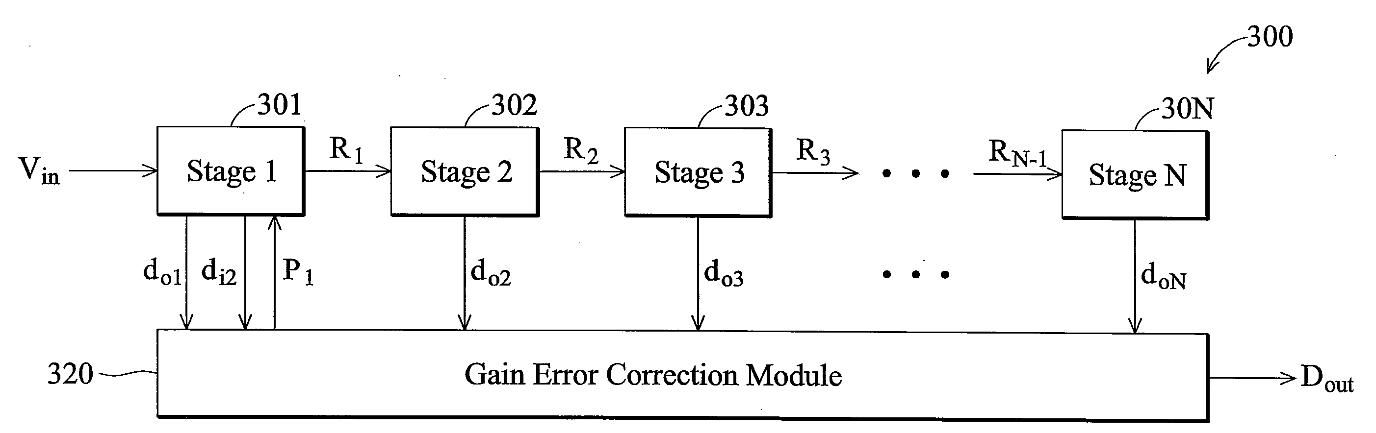
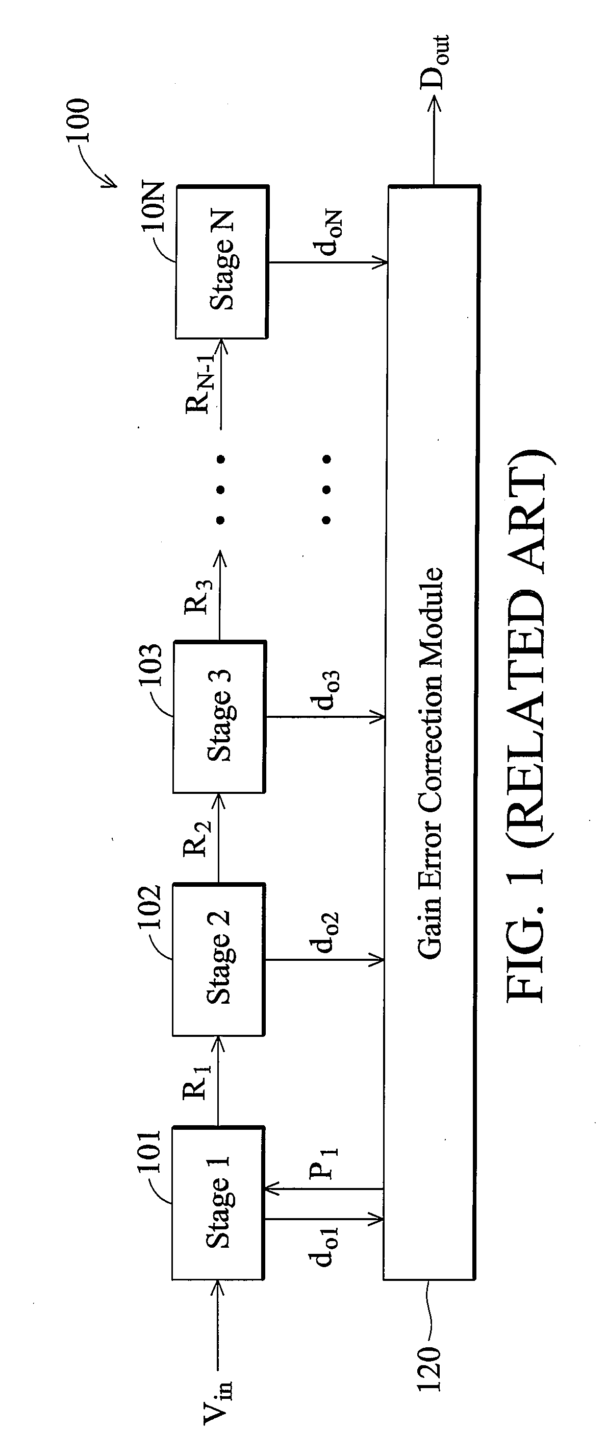
[0025]FIG. 3 is a block diagram of a pipelined ADC 300 implementing gain error estimation of a first stage 301 according to the invention. The pipelined ADC 300 is roughly similar to the pipelined ADC 100 of FIG. 1 with the exception of the first stage 301 and the gain error correction module 320. To estimate a gain error of the first stage 301, the gain error correction module 320 generates a correction number P1 fed to the first stage 301. After the first stage 301 generates a stage output value do1, the first stage 301 subtracts the stage output value do1 from its stage input signal Vin to obtain a residual signal, processes the residual signal according to the corr...


PUM


Abstract

The invention provides an analog-to-digital converter (ADC). The ADC comprises a plurality of stages connected in series, a gain error correction module, and a look-ahead module. Each of the stages derives a stage output value from a stage input signal and generates a stage output signal as the stage input signal of a subsequent stage, wherein one of the stages is selected as a target stage for estimating a gain value thereof. The gain error correction module delivers a correction number to the target stage to affect the stage output signal of the target stage and the stage output values of subsequent stages of the target stage, receives at least one auxiliary output value from a look-ahead module dedicated to the target stage, and derives an error estimate of the gain value of the target stage from the stage output values and the auxiliary output value. The look-ahead module generates the auxiliary output value according to the stage output value of the target stage, wherein the auxiliary output value is not affected by the correction number.

Description

CROSS REFERENCE TO RELATED APPLICATIONS[0001]This application claims the benefit of U.S. Provisional Application No. 60 / 981,254, filed on Jul. 23, 2007, the entirety of which is incorporated by reference herein.BACKGROUND OF THE INVENTION[0002]1. Field of the Invention[0003]The invention relates to analog-to-digital converters (ADC), and more particularly to gain error calibration of ADCs.[0004]2. Description of the Related Art[0005]An analog-to-digital converter converts an analog input signal to a digital output signal. Analog-to-digital converters are classified into several categories including flash ADCs, pipelined ADCs, and cyclic ADCs. Among the three ADC categories, a flash ADC has the shortest latency, because it has the simplest circuit structure. A flash ADC comprises multiple comparators directly comparing an analog input signal with multiple reference voltages to generate a digital output signal. When the required resolution of a digital output signal increases, a flash...

Claims


Application Information

Patent Timeline
IPC IPC(8): H03M1/10H03M1/12
CPCH03M1/1019H03M1/164H03M1/162
Inventor HSUEH, KANG-WEITU, YU-HSUAN
Owner MEDIATEK INC
Learn More