Unlock instant, AI-driven research and patent intelligence for your innovation.

Semiconductor memory

Active Publication Date: 2009-03-05
KIOXIA CORP
View PDF1 Cites 11 Cited by
  • Summary
  • Abstract
  • Description
  • Claims
  • Application Information

AI Technical Summary

Problems solved by technology

On the other hand, a large memory capacity of the NAND type flash memories is required due to multi-functions of the electronic devices, and thus the compatibility between shrink of memory cells and improvement in reliability becomes a problem (for example, see Jpn. Pat. Appln. KOKAI Publication Nos. 2002-184875, 5-88375 and 8-55920).
Such a problem arises not only in NAND type flash memories but also in other semiconductor memories where a large memory capacity is required.

Method used


Image

  • Semiconductor memory
  • Semiconductor memory
  • Semiconductor memory

Examples


first example

(1) First Example

[0085]A. Structure

[0086]FIG. 3 shows a main section of the NAND type flash memory.

[0087]j (j is any number not less than 2) blocks BK1, BK2, . . . , BKj are arranged in the second direction in the memory cell array 1. The blocks BK1, BK2, . . . , BKj have a plurality of NAND cell units which are arranged in the first direction, respectively.

[0088]The row decoder (word line driver) 2 selects selected one word line in selected one block BKi (i is one of 1 to j) at the time of reading / writing.

[0089]A data latch circuit 4 has a function for temporarily latching data at the time of reading / writing. The data latch circuit 4 is arranged on both endmost portions of the memory cell array area 1 in the second direction. This layout is effective for an ABL (all bit line) sense principle.

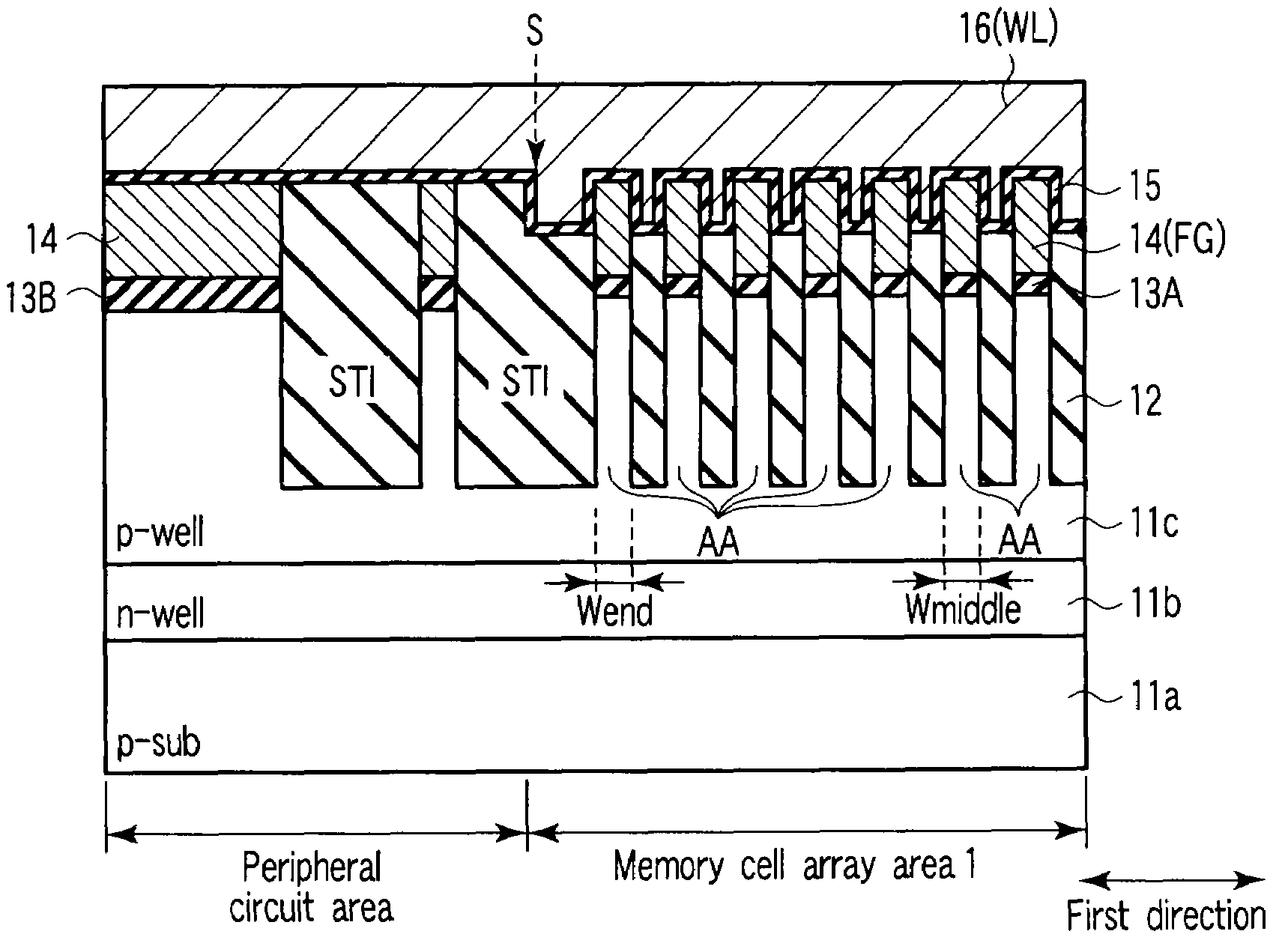
[0090]FIG. 4 is a plan view showing the memory cell array area. FIG. 5 is a cross-sectional view taken along line V-V of FIG. 4, and FIG. 6 is a cross-sectional view taken along line VI-VI of F...

second example

(2) Second Example

[0141]In contrast to the first example, a second example relates to the closed-loop structured active area where at least the first active area from the endmost portion in the first direction is arranged in the peripheral circuit area.

[0142]A. Structure

[0143]FIG. 24 is a plan view showing the memory cell array area. FIG. 25 is a cross-sectional view taken along line XXV-XXV of FIG. 24, and FIG. 26 is a cross-sectional view taken along line XXVI-XXVI of FIG. 24.

[0144]The double well region, which includes the n-type well region (n-well) 11b and the p-type well region (p-well) 11c, is formed in the p-type semiconductor substrate (p-sub) 11a.

[0145]In the memory cell array area 1, the active areas AA and the element isolation areas (areas other than the active areas AA) are arranged alternately in the first direction so as to form the periodical structure. The n-th (n is odd number) active area AA from the endmost portion in the first direction and the (n+1)-th active...

modification example

4. MODIFICATION EXAMPLE

[0200]Some modification examples of the present invention will be described.

[0201]The position of the step of the element isolation insulating film can be set between the (m−1)-th active area from the endmost portion in the first direction and the m-th active area in the second example. However, m is any number not less than 2.

[0202]For example as shown in FIGS. 44 and 45, the step may be set between the first active area AA from the endmost portion in the first direction and the second active area AA in the closed-loop structured active areas AA constituting the periodical structure.

[0203]FIGS. 44 and 45 correspond to FIGS. 40 and 43 in the above manufacturing method.

[0204]In this case, as is clear from FIG. 45, an opposed area between the conductive layer 14 and the control gate electrode 16 (WL) is small on the first active area AA from the endmost portion in the first direction. As a result, the capacitance of the capacitor (corresponding to C2 in FIG. 41)...


PUM


Abstract

A semiconductor memory according to an example of the invention includes active areas, and element isolation areas which isolate the active areas. The active areas and the element isolation areas are arranged alternately in a first direction. An n-th (n is odd number) active area from an endmost portion in the first direction and an (n+1)-th active area are coupled to each other at an endmost portion in a second direction perpendicular to the first direction.

Description

CROSS-REFERENCE TO RELATED APPLICATIONS[0001]This application is based upon and claims the benefit of priority from prior Japanese Patent Application No. 2007-222783, filed Aug. 29, 2007, the entire contents of which are incorporated herein by reference.BACKGROUND OF THE INVENTION[0002]1. Field of the Invention[0003]The present invention relates to an active area structure of a memory cell array.[0004]2. Description of the Related Art[0005]In recent years, many electronic devices which use NAND type flash memories have been commercially available. On the other hand, a large memory capacity of the NAND type flash memories is required due to multi-functions of the electronic devices, and thus the compatibility between shrink of memory cells and improvement in reliability becomes a problem (for example, see Jpn. Pat. Appln. KOKAI Publication Nos. 2002-184875, 5-88375 and 8-55920).[0006]For example, a memory cell array of the NAND type flash memories has a periodical structure in which ...

Claims


Application Information

Patent Timeline
IPC IPC(8): H01L27/105
CPCH01L27/0207H01L27/105H01L27/11526H01L27/11534H01L2924/0002H01L2924/00H10B41/43H10B41/40
Inventor IZUMI, TATSUOKAMIGAICHI, TAKESHITAKAHASHI, SHINYA
Owner KIOXIA CORP
Features
  • R&D
  • Intellectual Property
  • Life Sciences
  • Materials
  • Tech Scout
  • Unparalleled Data Quality
  • Higher Quality Content
  • 60% Fewer Hallucinations
Learn More