Light emitting diode package structure

Inactive Publication Date: 2009-03-26
YEH HSIN HUI
View PDF0 Cites 1 Cited by
  • Summary
  • Abstract
  • Description
  • Claims
  • Application Information

AI Technical Summary

Benefits of technology

[0008]According to the problems described above, the main object of the present invention is to provide a transparent substrate to package with the light emitting diode (LED) at the same time and shorten the LED package time to reduce the process period and cut the package cost.
[0009]The other object of the present invention is to connect the LED with the transparent substrate and increase the liability of the elements.

Problems solved by technology

But how to enhance the extraction efficiency of the LED package structure to get higher overall efficiency in the quantum efficiency inside the semiconductor chip of the LED is the important issue in current technology.

Method used


Image

  • Light emitting diode package structure
  • Light emitting diode package structure
  • Light emitting diode package structure

Examples


Embodiment Construction

[0024]The following detailed description of the present invention describes a light emitting diode package structure necessary to provide an understanding of the present invention, but does not cover a complete structure composition and the operating theory. The portions relating to the conventional techniques are briefly described, and the parts of the drawings are not proportionally drafted. While embodiments are discussed, it is not intended to limit the scope of the present invention. Except expressly restricting the amount of the components, it is appreciated that the quantity of the disclosed components may be greater than that disclosed.

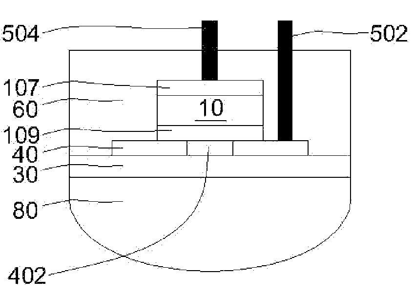
[0025]First of all, please referring to FIG. 1; it is a view showing that the light emitting diode (LED) structure of the present invention. The LED structure 10 includes a semiconductor layer 103 with light emitting function. There are an N electrode 107 and a P electrode 109 disposed on the two sides of the semiconductor layer 103. The LED s...


PUM


Abstract

The present invention provides a light emitting diode (LED) package, which includes a carrier substrate having a first surface and a second surface; a metal layer formed in the first surface of the carrier substrate, and a through hole formed in the central area of the metal layer to expose the portion of the first surface of the carrier substrate; a LED having a semiconductor layer capable of light emitting, and an N electrode and a P electrode on the two sides of the semiconductor layer, in which P electrode is electrically connected to the first surface of the metal layer; a first connecting element is electrically connected to the metal layer; a second connecting element is electrically connected to the N electrode; and an encapsulated material is formed to cover the LED, the metal layer, the exposed first connecting element and the second connecting element.

Description

BACKGROUND OF THE INVENTION[0001]1. Field of the Invention[0002]The present invention is a light emitting diode (LED) package structure and more particularly is a package structure that the LED is electrically connected to a metal layer on a transparent substrate.[0003]2. Description of the Prior Art[0004]Light emitting diode (LED) is widely used in any electronic devices and is more popular in the industry. The energy consumption of the LED is lower than the conventional incandescent lamp or fluorescent lamp and the size of the LED is smaller than the conventional lamp. Therefore, the demand of the LED is increased day after day because the trend of the size of the electronic products is smaller and smaller.[0005]LED is a light emitting element used to directly transform the electrical power to light power without the heating and luminescent procedure of transforming the electrical power to heat power. Therefore, LED is also called the luminescence emitting element. LED not only in...

Claims


Application Information

Patent Timeline
IPC IPC(8): H01L33/00H01L33/54H01L33/56
CPCH01L33/56H01L33/54H01L2924/181H01L2224/16225H01L2224/97H01L2924/00012
Inventor YEH, HSIN-HUI
Owner YEH HSIN HUI
Why Eureka
Try Eureka