Methods and Systems for Forming at Least One Dielectric Layer
- Summary
- Abstract
- Description
- Claims
- Application Information
AI Technical Summary
Problems solved by technology
Method used
Image

Examples
Example
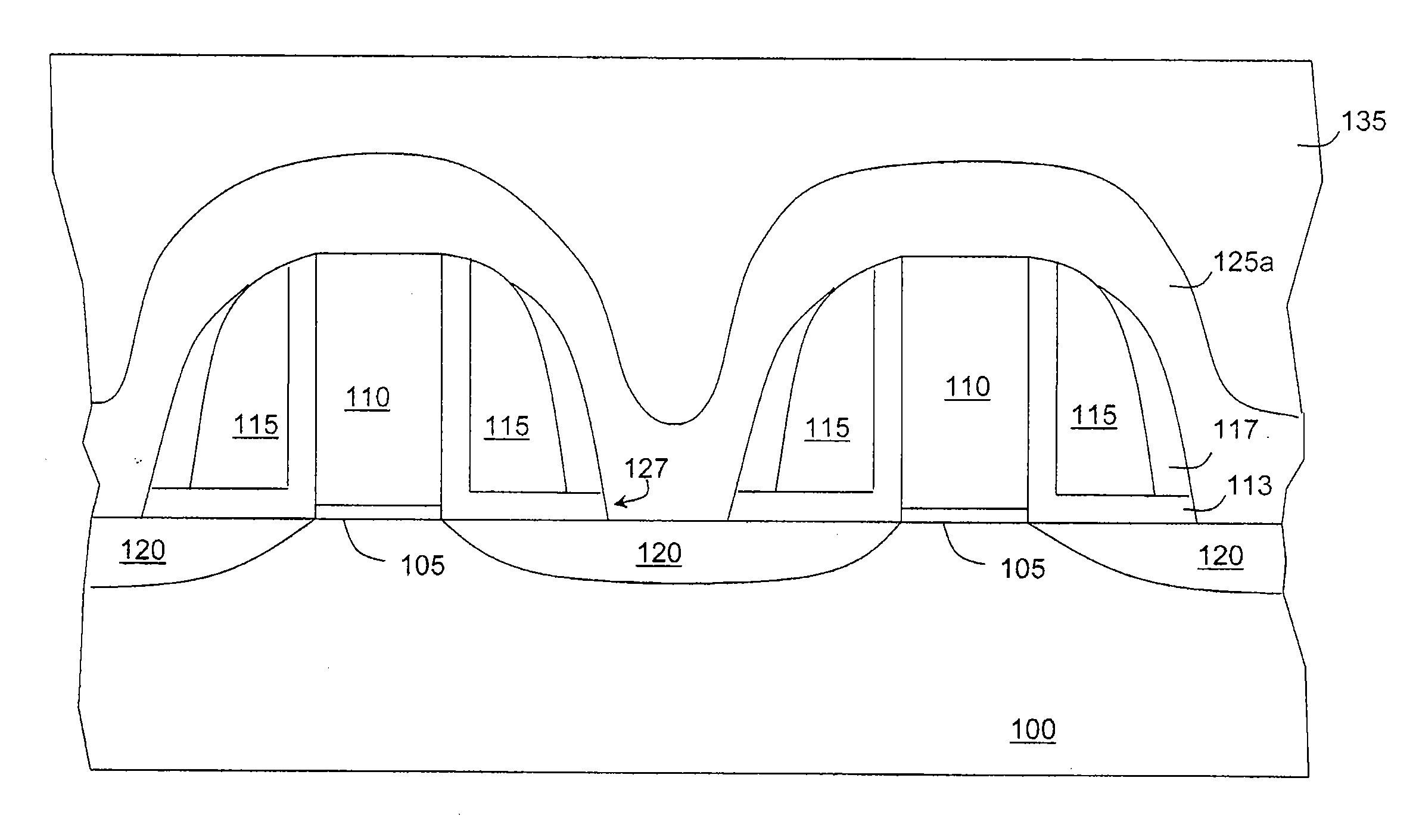
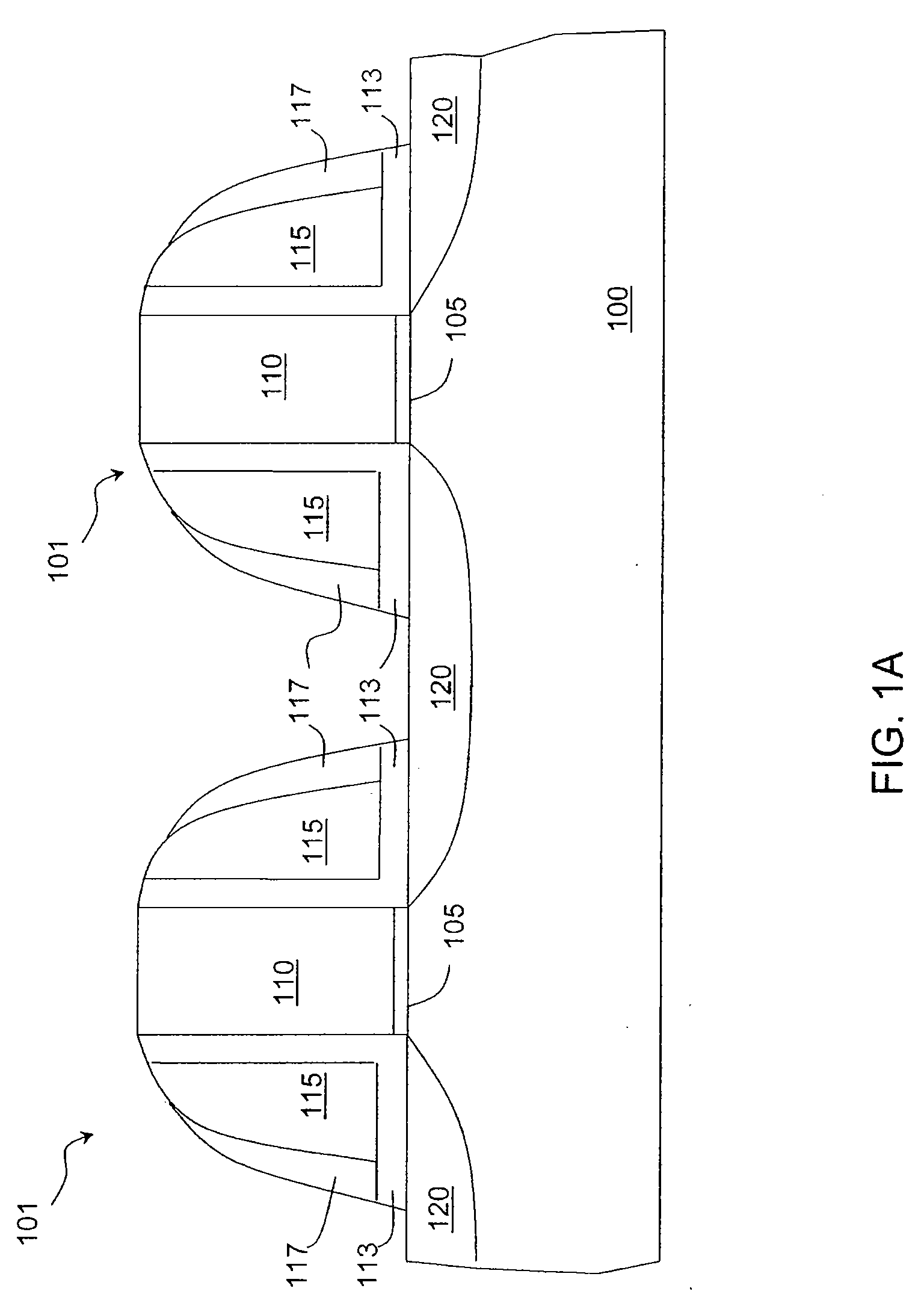
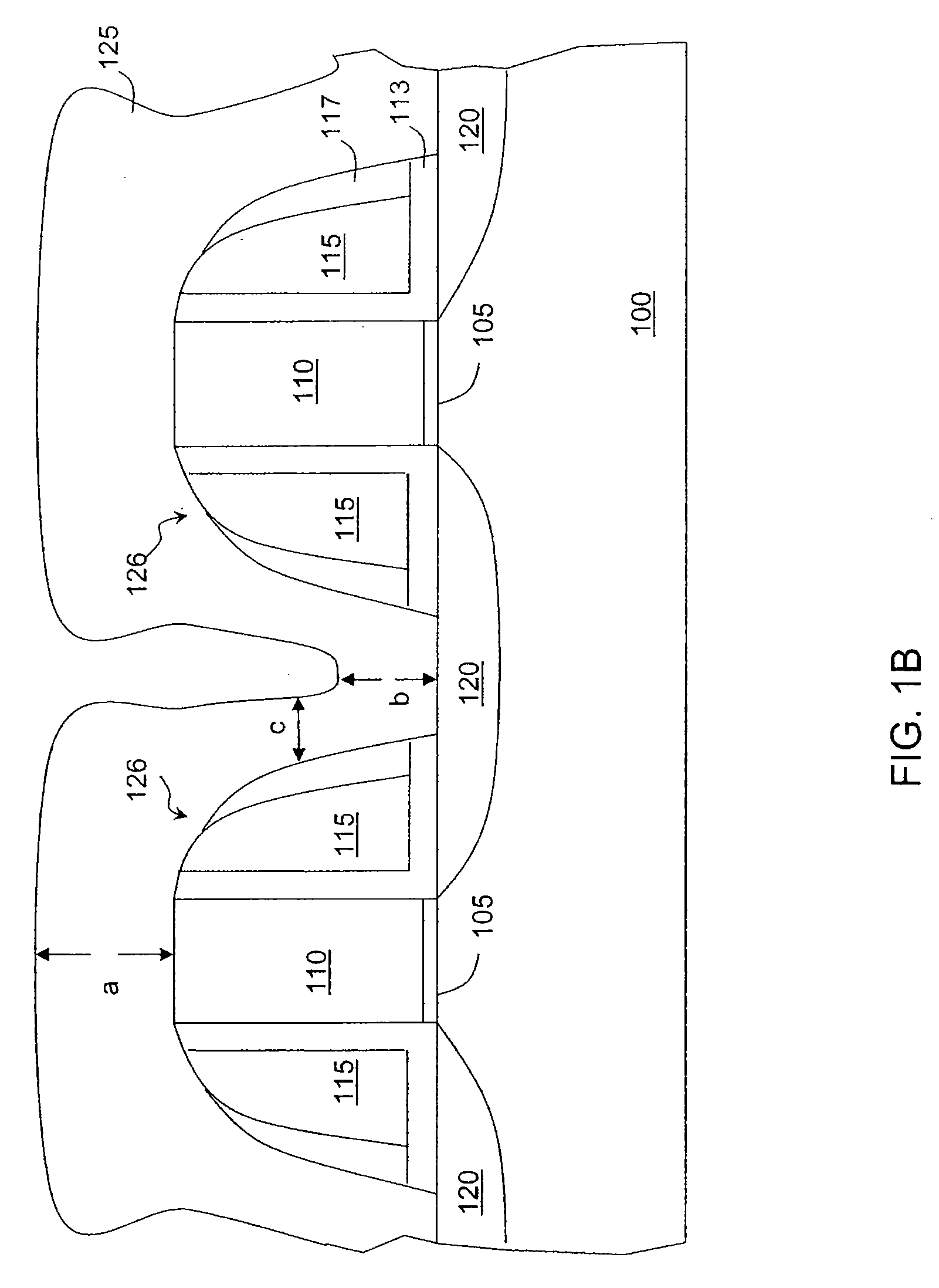
[0019]Systems and methods are described for forming at least one dielectric layer over at least one feature, e.g., transistor gate, formed across a surface of a substrate. The dielectric layer is subjected to an etch process. The etch process may desirably reduce aspect ratio gaps and / or trenches (e.g., aspect ratios of about 5:1 or more). A dielectric layer then may be formed over the etched dielectric layer, such that the aspect ratio gaps and / or trenches may be filled with dielectric materials substantially without gaps or seams.
[0020]The methods of the invention include forming at least one feature across a surface of a substrate. A dielectric layer is formed over the at least one feature. A first portion of the dielectric layer around the corner of the feature is removed at a first rate and a second portion of the dielectric layer over the substrate adjacent to a bottom region of the at least one feature is removed at a second rate. The first rate is greater than the second rat...
PUM
| Property | Measurement | Unit |
|---|---|---|
| Temperature | aaaaa | aaaaa |
| Temperature | aaaaa | aaaaa |
| Temperature | aaaaa | aaaaa |
Abstract
Description
Claims
Application Information
 - R&D Engineer
- R&D Manager
- IP Professional
- Industry Leading Data Capabilities
- Powerful AI technology
- Patent DNA Extraction
Browse by: Latest US Patents, China's latest patents, Technical Efficacy Thesaurus, Application Domain, Technology Topic.
© 2024 PatSnap. All rights reserved.Legal|Privacy policy|Modern Slavery Act Transparency Statement|Sitemap