Wafer and method of forming alignment markers
a technology of alignment markers and wafers, applied in the field of multilayer structures, can solve the problems of less wafer revenue, reduced available space on the wafer for circuits,
- Summary
- Abstract
- Description
- Claims
- Application Information
AI Technical Summary
Problems solved by technology
Method used
Image
Examples
Embodiment Construction
[0016]Throughout the following description identical reference numerals will be used to identify like parts.
[0017]The example described herein is generally applicable to multi-layer structures that are susceptible to cracking, particularly as a result of the presence of metallisation layers, such as copper metallisation layers.
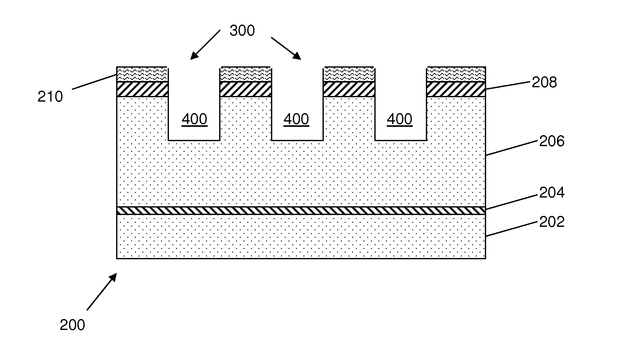
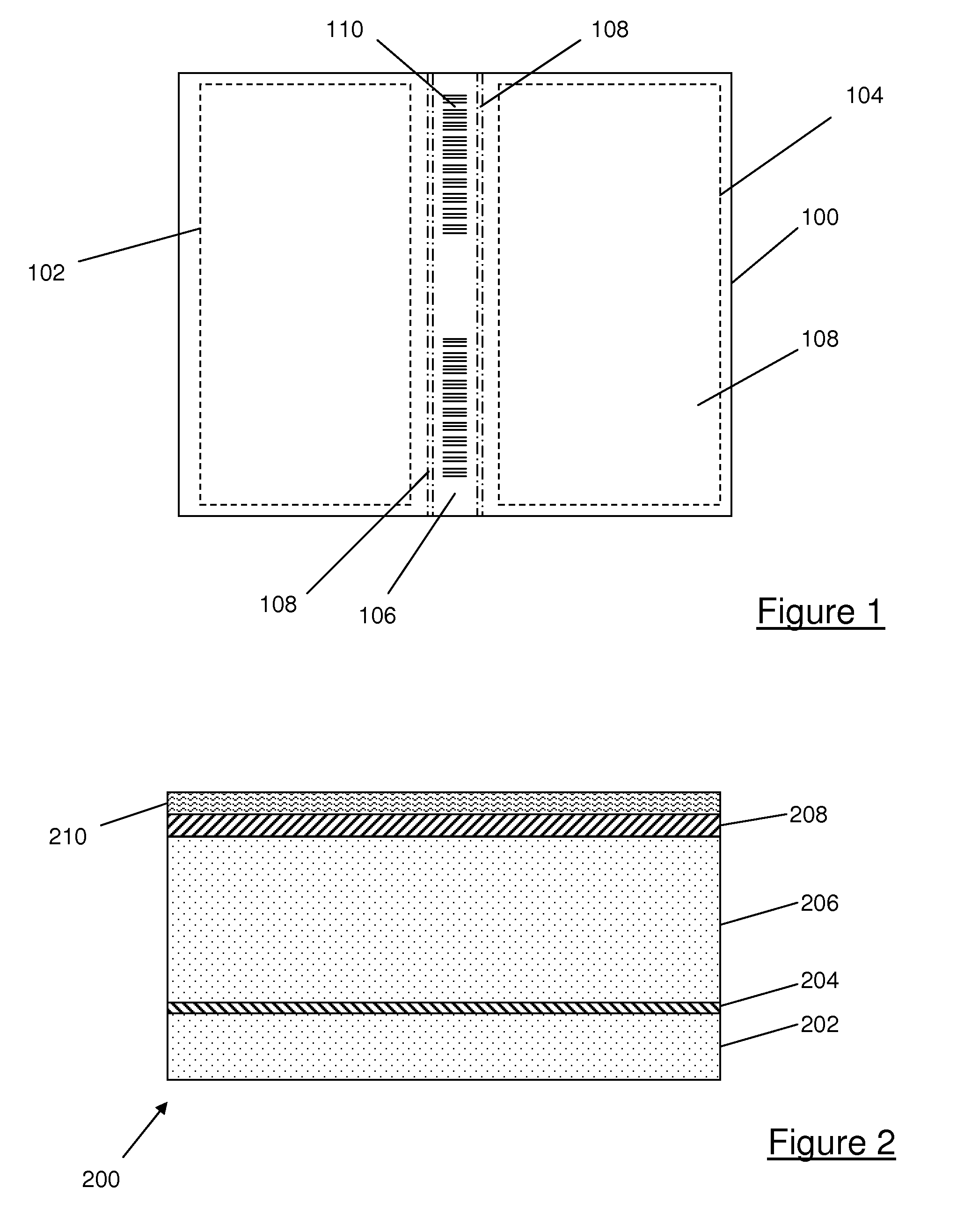
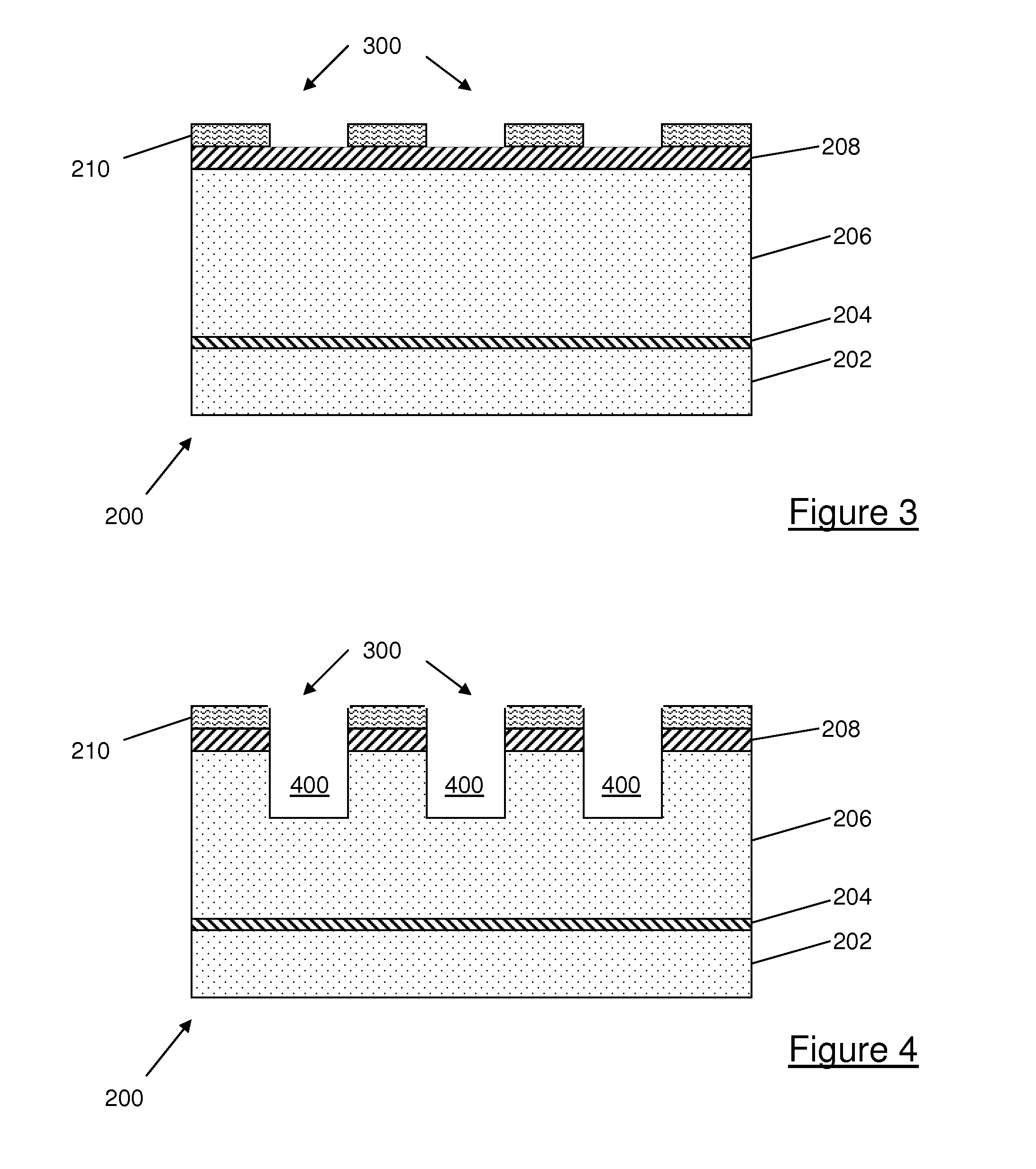
[0018]In order to fabricate a number of semiconductor devices, a semiconductor substrate has a number of different layers of materials formed thereon, thereby constituting a multi-layer structure. Each layer of the multi-layer structure has a distinct pattern, depending upon the semiconductor devices being formed. The distinct pattern of each layer of the multi-layer structure is achieved using any suitable patterning technique known in the art.
[0019]Typically, latter stages of semiconductor device fabrication, sometimes referred to as the “back end” of the processing, are metallisation stages where electrical contacts between layers of the multi-layer structu...
PUM
 Abstract
Description
Claims
Application Information


