Semiconductor automation buffer storage identification system and method

Inactive Publication Date: 2009-07-16
TAIWAN SEMICON MFG CO LTD
View PDF16 Cites 0 Cited by
  • Summary
  • Abstract
  • Description
  • Claims
  • Application Information

AI Technical Summary

Problems solved by technology

However, it sometimes occurs that the control system of the semiconductor manufacturing facility is rendered blind as to the specific location of each substrate carrier.
This can occur when the data provided to the control system is lost or corrupted.
This process is very time consuming and represents time that the facility is not processing wafers, which is, of course, very costly.
If an entire fabrication facility with 5000 buffer locations needs to have the substrate carriers read, this can mean that all of the OHTs will be tied up in identifying the substrate carriers instead of delivering product to the processing tools, creating a potential bottleneck for the facility.

Method used


Image

  • Semiconductor automation buffer storage identification system and method
  • Semiconductor automation buffer storage identification system and method
  • Semiconductor automation buffer storage identification system and method

Examples


Embodiment Construction

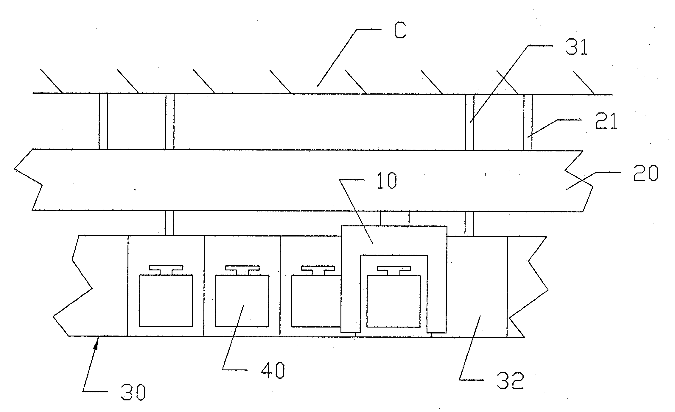
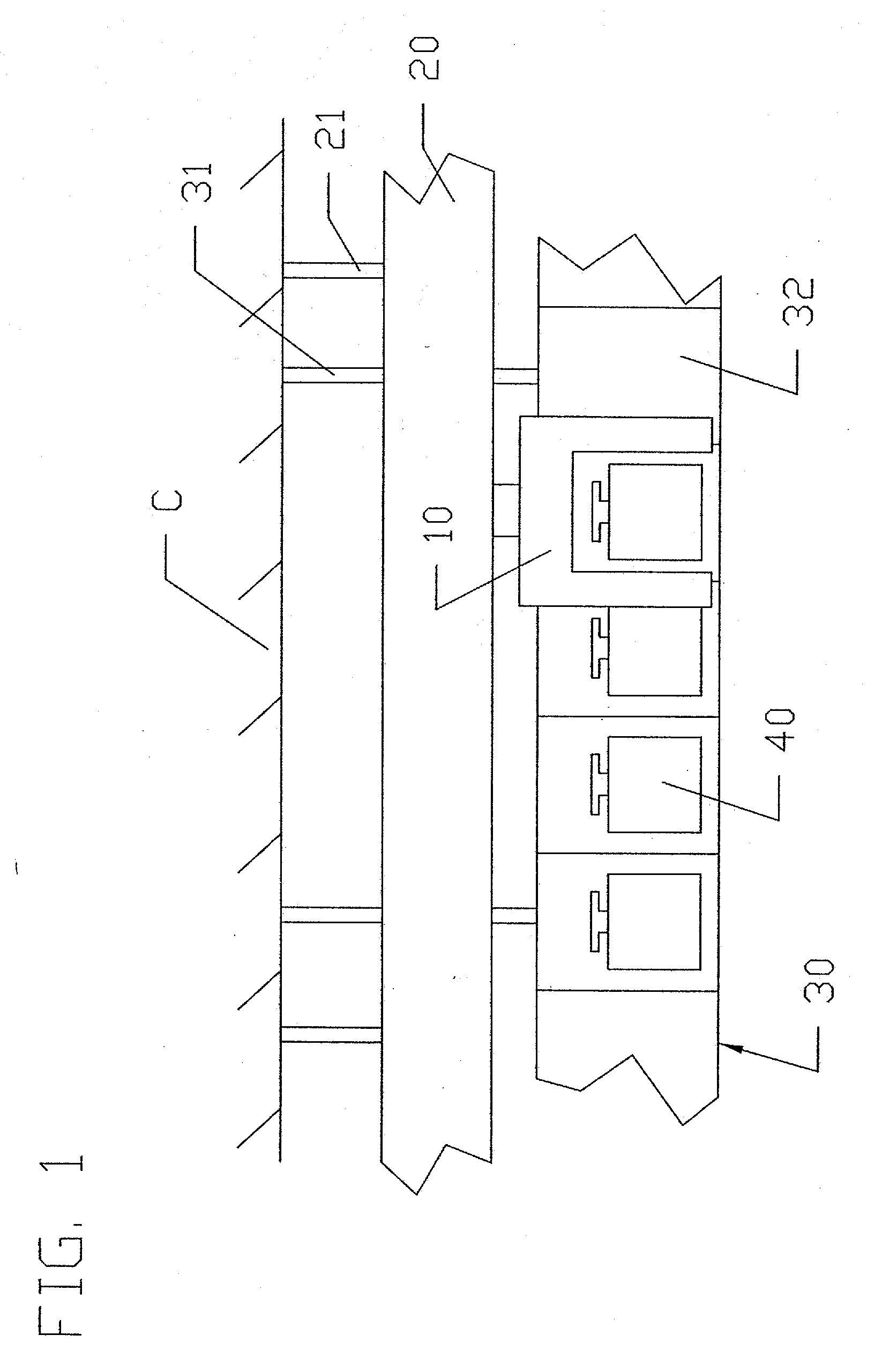
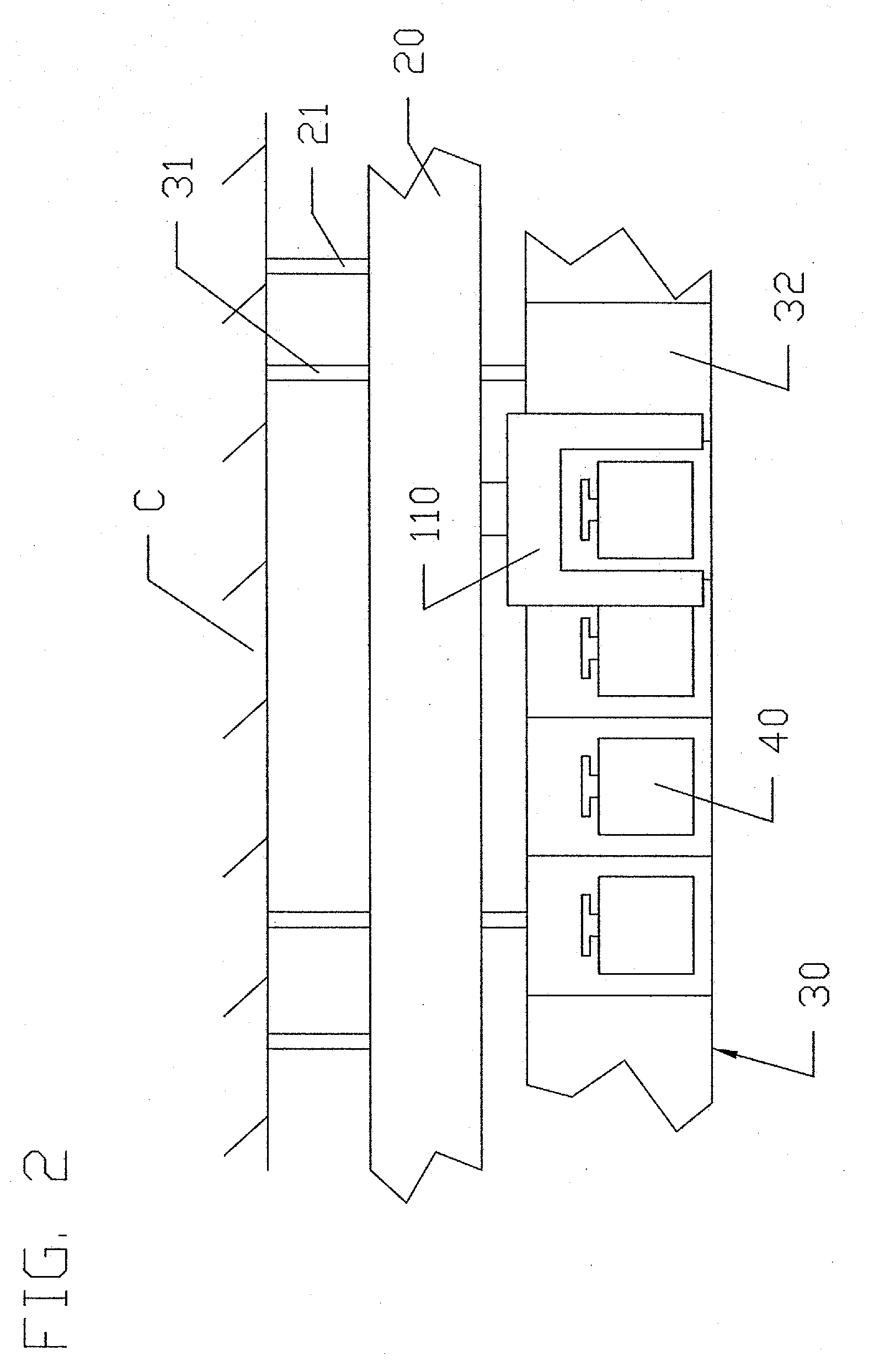
[0023]The invention generally relates to an overhead transport vehicle (OHT) which can be used in a semiconductor manufacturing environment or facility and which can read substrate carriers and / or wafers arranged therein. Substrate carriers are also known as front opening unified pods (FOUPs), standard mechanical interface (SMIF) pods, and cassettes. The invention also relates to a system and method for reading substrate carriers, and / or wafers arranged therein (e.g., in the case where a dummy wafer arranged in the FOUP includes an RFID tag), arranged in a buffer storage of a semiconductor manufacturing environment or facility using the OHT. The reading can preferably occur as the OHT passes the substrate carriers arranged in the overhead buffer storage system.

[0024]The invention offers a significant improvement over known systems of reading of the substrate carriers. For example, in an Annex East Phase having 206 buffer storage locations in three different bays, according to the in...


PUM


Abstract

A system for reading substrate carriers that includes at least one overhead transport vehicle (OHT) utilizing at least one device for at least one of sensing and / or reading a substrate carrier, and / or wafers arranged therein, when the substrate carrier is proximate the at least one overhead transport vehicle. A method of sensing or reading a substrate carrier includes sensing and / or reading a substrate carrier and / or wafers arranged therein with the overhead transport vehicle.

Description

FIELD OF THE INVENTION[0001]The invention generally relates to a system and method for reading substrate carriers, and / or wafers arranged therein, arranged in a buffer storage of a semiconductor manufacturing environment or facility using an overhead transport vehicle.BACKGROUND OF THE INVENTION[0002]Semiconductor manufacturing facilities typically utilize a number of buffer storage areas, a number of bays that includes processing tools, an overhead track system, and a number of overhead traveling vehicles or transporters (OHTs). The buffer storage areas store substrate carriers which are also known as front opening unified pods (FOUPs), standard mechanical interface (SMIF) pods, and cassettes.[0003]It is also known to utilize overhead buffer storage systems (aka zero footprint storage) in semiconductor manufacturing facilities. These overhead storage systems are typically suspended from a ceiling in a manner similar to the track system. An OHT can access the overhead buffer storage...

Claims


Application Information

Patent Timeline
IPC IPC(8): B66C19/00
CPCH01L21/67294H01L21/67769H01L21/67733H01L21/6773Y10S414/14
Inventor CAMPBELL, PHILIP L.JOE, DENISE B.SHERWOOD, EDWARD
Owner TAIWAN SEMICON MFG CO LTD
Why Eureka
Try Eureka