Vertical organic fet and method for manufacturing same

a vertical organic and fet technology, applied in the direction of semiconductors, electrical devices, transistors, etc., can solve the problems of slow operation and low carrier mobility, and achieve the effect of improving carrier mobility and operating characteristics

Inactive Publication Date: 2009-07-16
PANASONIC CORP
View PDF13 Cites 3 Cited by
  • Summary
  • Abstract
  • Description
  • Claims
  • Application Information

AI Technical Summary

Problems solved by technology

However, if a horizontal type is merely turned around into vertical type, since the molecular orientation is parallel to the substrate as mentioned above, or in other words, is perpendicular to a straight line connecting the source and drain, this structure leads to lower carrier mobility and slower operation than with a vertical organic FET.

Method used


Image

  • Vertical organic fet and method for manufacturing same
  • Vertical organic fet and method for manufacturing same
  • Vertical organic fet and method for manufacturing same

Examples


example 1

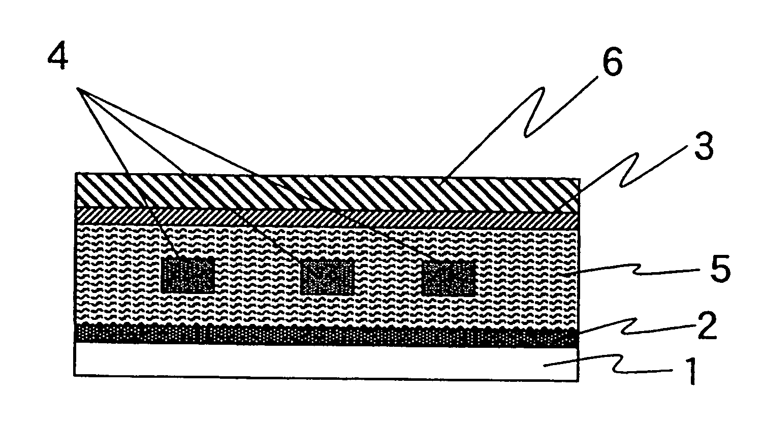
[0127]FIG. 6 illustrates a test example of the present invention. A film was formed in a thickness of 80 nm and a width of 1 mm from gold (source electrode layer 20) on a quartz substrate 10 by vacuum vapor deposition. A film of an organic compound (SnCl2-Pc; active layer 50) was then formed in a thickness of 100 nm at a vapor deposition rate of 0.1 nm / sec, a substrate temperature of room temperature, and a degree of vacuum of 10−4 Pa. Then, aluminum was used to form gate electrodes 40 in a thickness of 50 nm and a spacing of 30 μm by vacuum vapor deposition, and this product was exposed to the air. After this, an active layer 50 was again formed in a thickness of 100 nm under the same conditions as above, over which gold (drain electrode layer 30) was vapor deposited in a thickness of 80 nm, which produced a vertical organic FET. The FET characteristics were evaluated under an inert atmosphere, the source and drain currents were modulated by gate voltage application, and the FET op...


PUM


Abstract

The present invention provides a vertical organic FET with increased carrier mobility and suppressed molecular orientation of an active layer composed of an organic semiconductor. The present invention relates to a vertical organic FET having a structure in which at least a source electrode layer, a drain electrode layer, a gate electrode, and an active layer are provided on a substrate, and the source electrode layer, the active layer, and the drain electrode layer are laminated in that order, wherein (1) the source electrode layer and the drain electrode layer are disposed substantially parallel to the substrate plane, (2) the source electrode layer and the drain electrode layer are electroconductive members, (3) the active layer is substantially constituted by a phthalocyanine compound that has a tetravalent or hexavalent element as its central atom and in which ligands X1 and X2 coordinate up and down, respectively, from the molecular plane, and (4) the compound is layered such that the molecular plane of each molecule of the compound is in a substantially parallel state with respect to the source electrode layer and / or the drain electrode layer.

Description

FIELD OF THE INVENTION[0001]This invention relates to a novel vertical organic FET and a method for manufacturing the same.BACKGROUND OF THE INVENTION[0002]Recent years have seen research into the use of organic semiconductor materials as active layers in a variety of devices, such as light emitting diodes, non-linear optical devices, and field effect transistors.[0003]Because they lend themselves so well to being worked, organic semiconductor materials allow for simpler and lower cost manufacturing equipment. Another advantage of organic semiconductor materials is that they can be laminated more easily than amorphous silicon or the like on a flexible plastic substrate.[0004]Most of the research conducted in the past into FETs made from organic semiconductor materials related to horizontal types. In these types, a gate electrode and an insulating layer are provided on a substrate, source and drain metal electrodes are disposed on top of the insulating layer, and an organic semicondu...

Claims


Application Information

Patent Timeline
Patent Type & Authority Applications(United States)
IPC IPC(8): H01L51/30H01L29/78H01L29/786H01L51/00
CPCH01L51/0078H01L51/057H01L51/0508H10K85/311H10K10/46H10K10/491
Inventor MIYAMOTO, AKIHITO
Owner PANASONIC CORP
Why Eureka
Try Eureka