Perforated Substrates for Forming Housings

a technology of perforated substrates and forming housings, which is applied in the direction of casings/cabinets/drawers, casings/cabinets/drawers details, electric apparatus casings/cabinets/drawers, etc., can solve the problems of cosmetic quality of metal parts, and affecting the appearance of metal parts

Active Publication Date: 2009-10-22
APPLE INC
View PDF44 Cites 61 Cited by
  • Summary
  • Abstract
  • Description
  • Claims
  • Application Information

AI Technical Summary

Problems solved by technology

Utilizing a welding process to attach internal features to metal parts is limiting in terms of the number and the complexity of the internal features that is possible using a welding technique.
Furthermore, the cosmetic quality of a metal part may be degraded as a result of a welding process.
As such, the presence of an undercut on the side of the metal sheet may be aesthetically undesirable, e.g., when the metal sheet is arranged to serve a cosmetic purpose.

Method used


Image

  • Perforated Substrates for Forming Housings
  • Perforated Substrates for Forming Housings
  • Perforated Substrates for Forming Housings

Examples


Embodiment Construction

[0025]Exemplary embodiments of the present invention are discussed below with reference to the various figures. However, those skilled in the art will readily appreciate that the detailed description given herein with respect to these figures is for explanatory purposes, as the invention extends beyond these embodiments.

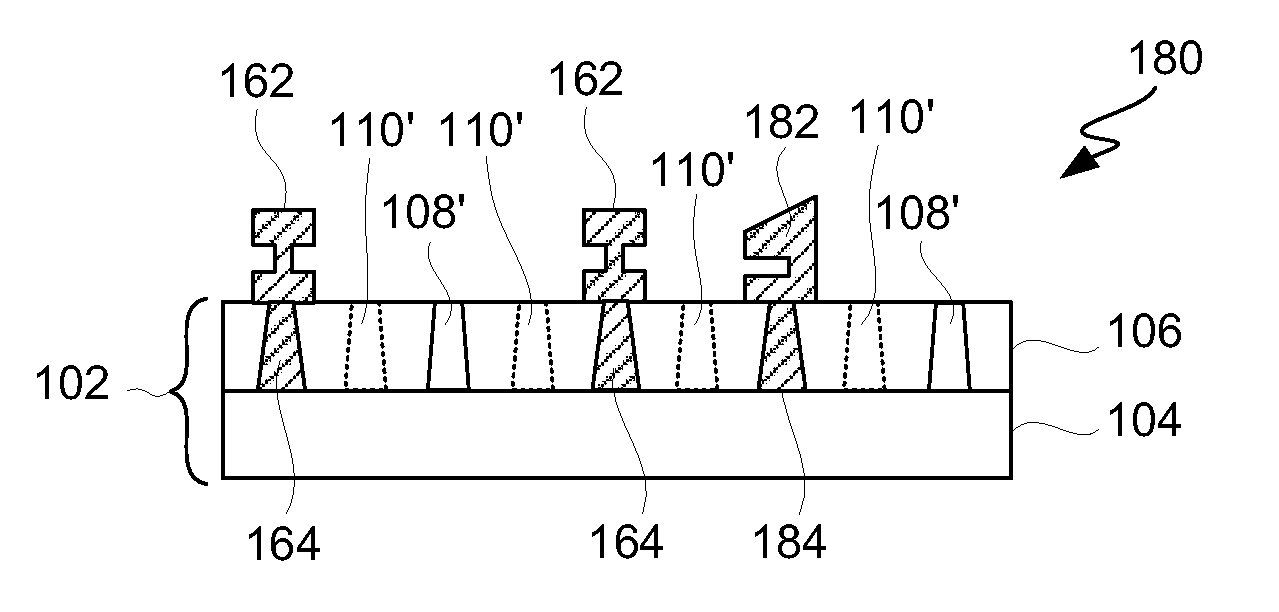
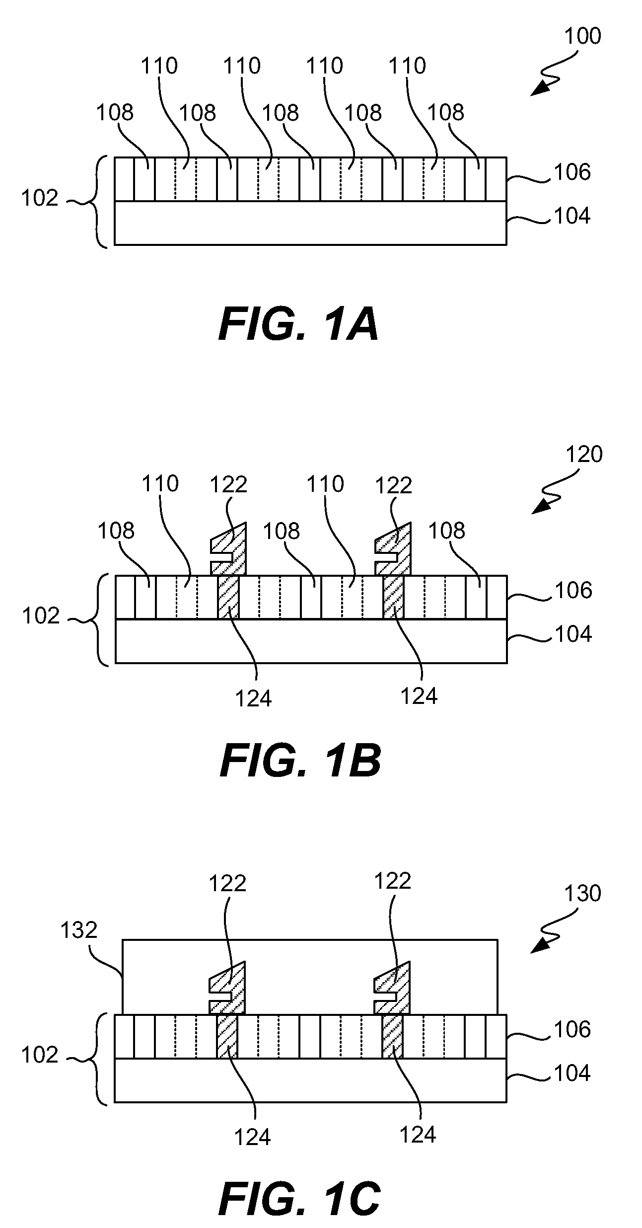
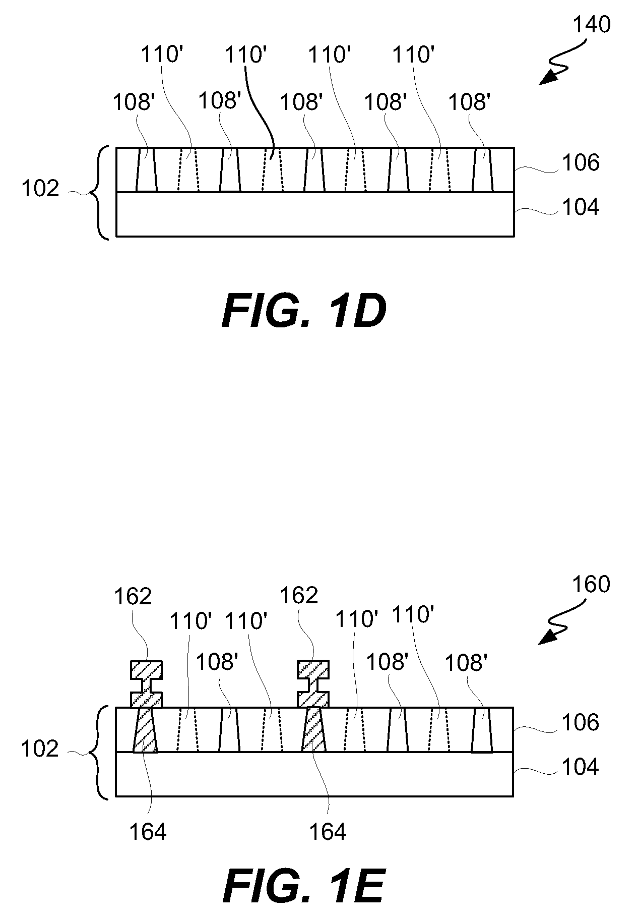
[0026]The invention pertains to a housing for an electronic device as well as methods for forming the housing. The housing can be formed from a substrate (material) having perforations to assist in adhering components internal to the housing. The substrate is typically a multi-layer substrate having at least two layers. In one embodiment, an inner layer of the multi-layer substrate can be provided with perforations. The perforations can them be used to adhere internal features (e.g., internal structures or attachment structures) to the multi-layer substrate. The internal features can be used for attaching parts or components to the multi-layer substrate, thereby secu...


PUM

PropertyMeasurementUnit
diameteraaaaaaaaaa
diameteraaaaaaaaaa
mechanical structuresaaaaaaaaaa

Abstract

A housing for an electronic device as well as methods for forming the housing are disclosed. The housing can be formed from a substrate having perforations to assist in adhering components internal to the housing. The substrate is typically a multi-layer substrate having at least two layers. In one embodiment, an inner layer of the multi-layer substrate can be provided with perforations. The perforations can them be used to adhere internal features to the multi-layer substrate. The internal features can be used for attaching parts or components to the multi-layer substrate, thereby securing the parts or components to the multi-layer substrate and thus the housing.

Description

CROSS-REFERENCE TO RELATED APPLICATION[0001]This application claims priority to U.S. Provisional Patent Application No. 61 / 046,260, filed Apr. 18, 2008, entitled “Perforated Substrates for Forming Housings”, which is herein incorporated herein by reference.BACKGROUND OF THE INVENTION[0002]1. Field of the Invention[0003]The present invention relates to forming housing for electronic devices.[0004]2. Description of the Related Art[0005]The manufacture of devices that include metal parts often includes the formation of features, e.g., complex mechanical structures, on surfaces of the metal parts. In order to ensure the structural integrity of such features, the features are often affixed to the surfaces of the metal parts using an adhesive material. By way of example, an internal feature has been obtained and glued in an appropriate location on a surface of a metal parts or housings.[0006]Alternatively, internal features have been welded to the surface of metal parts or housings. Utili...

Claims


Application Information

Patent Timeline
Patent Type & Authority Applications(United States)
IPC IPC(8): H05K7/14B32B3/06B32B37/02B32B3/10B21D51/16C23F1/02H05K5/00
CPCY10T29/4998Y10T428/24008H05K5/0217B32B2553/00B29K2705/00B32B38/04B29C45/1657H05K5/02B29C45/1671B29C45/14811B29C45/14311Y10T428/24289B29L2031/3481B32B2457/00B32B37/02B23P19/04B32B2038/047B29C45/14344B29C2045/14327
Inventor WEBER, DOUGLAS
Owner APPLE INC
Why Eureka
Try Eureka