Semiconductor memory device and control method thereof

a memory device and semiconductor technology, applied in the direction of information storage, static storage, digital storage, etc., can solve the problems of complicated control by a controller, inconvenient storage of drams, and limit to lowering power consumption, so as to avoid data destruction, avoid data destruction, and secure compatibility with drams

US20090268514A1Inactive Publication Date: 2009-10-29LONGITUDE LICENSING LTD
12 Cites 10 Cited by

Patent Information

Authority / Receiving Office
US · United States
Current Assignee / Owner
Publication Date
2009-10-29
Estimated Expiration
Not applicable · inactive patent

Smart Images

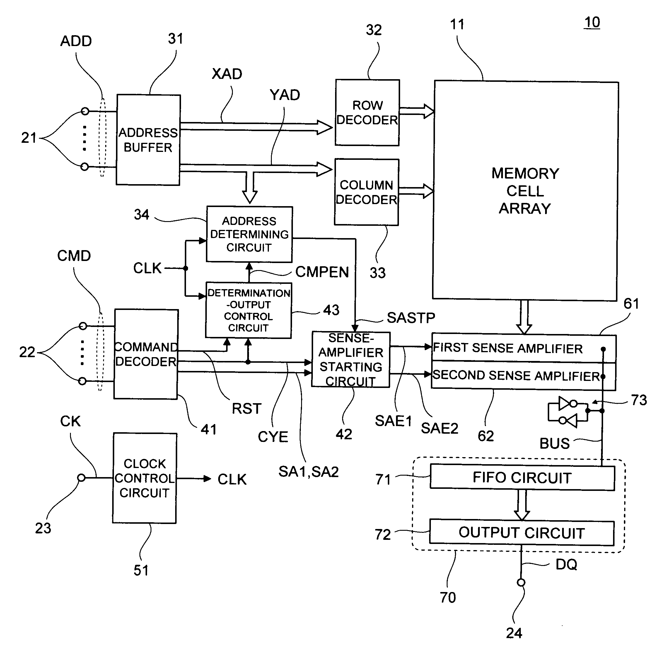
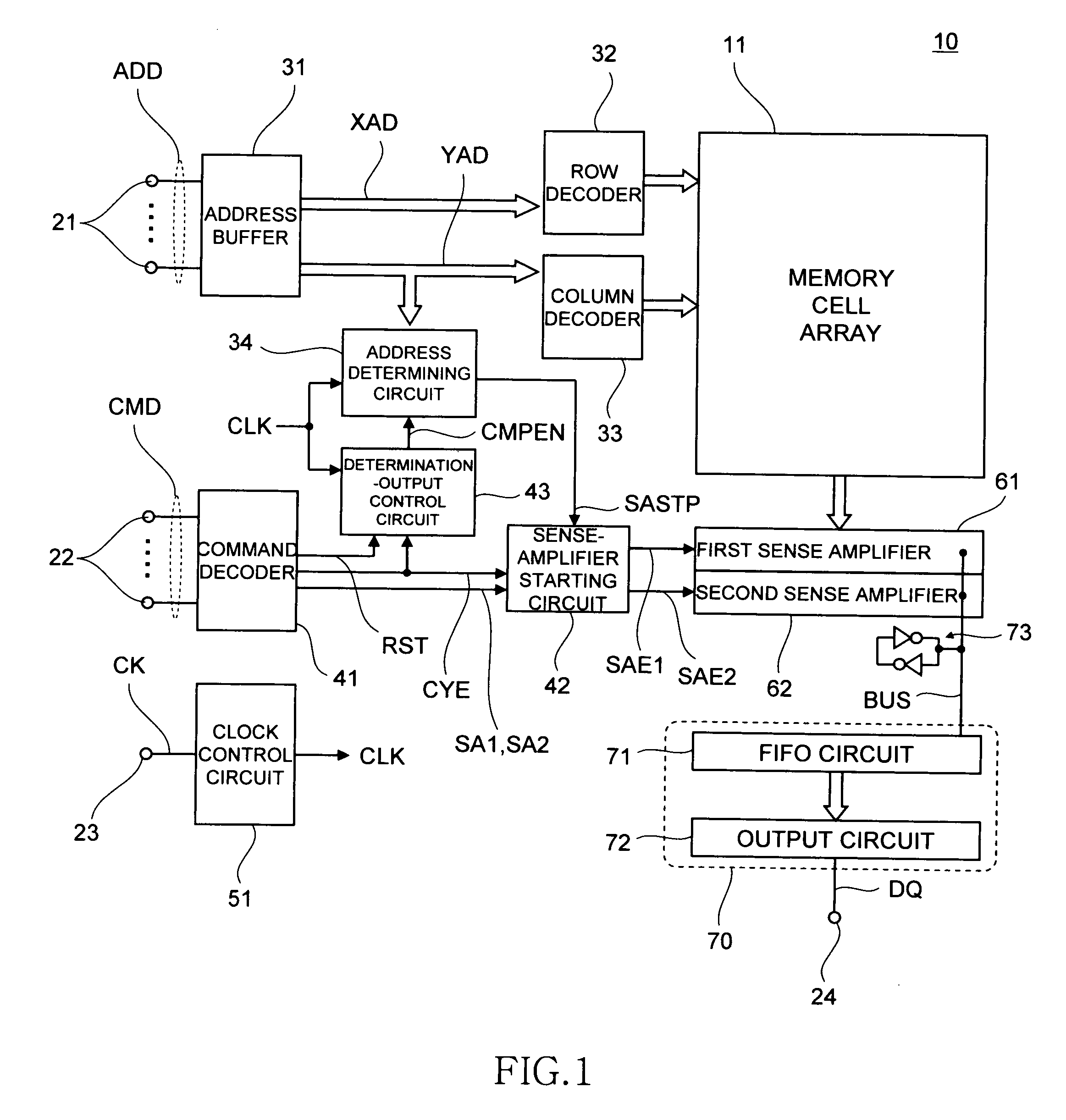
  • Figure 1
    Figure 1
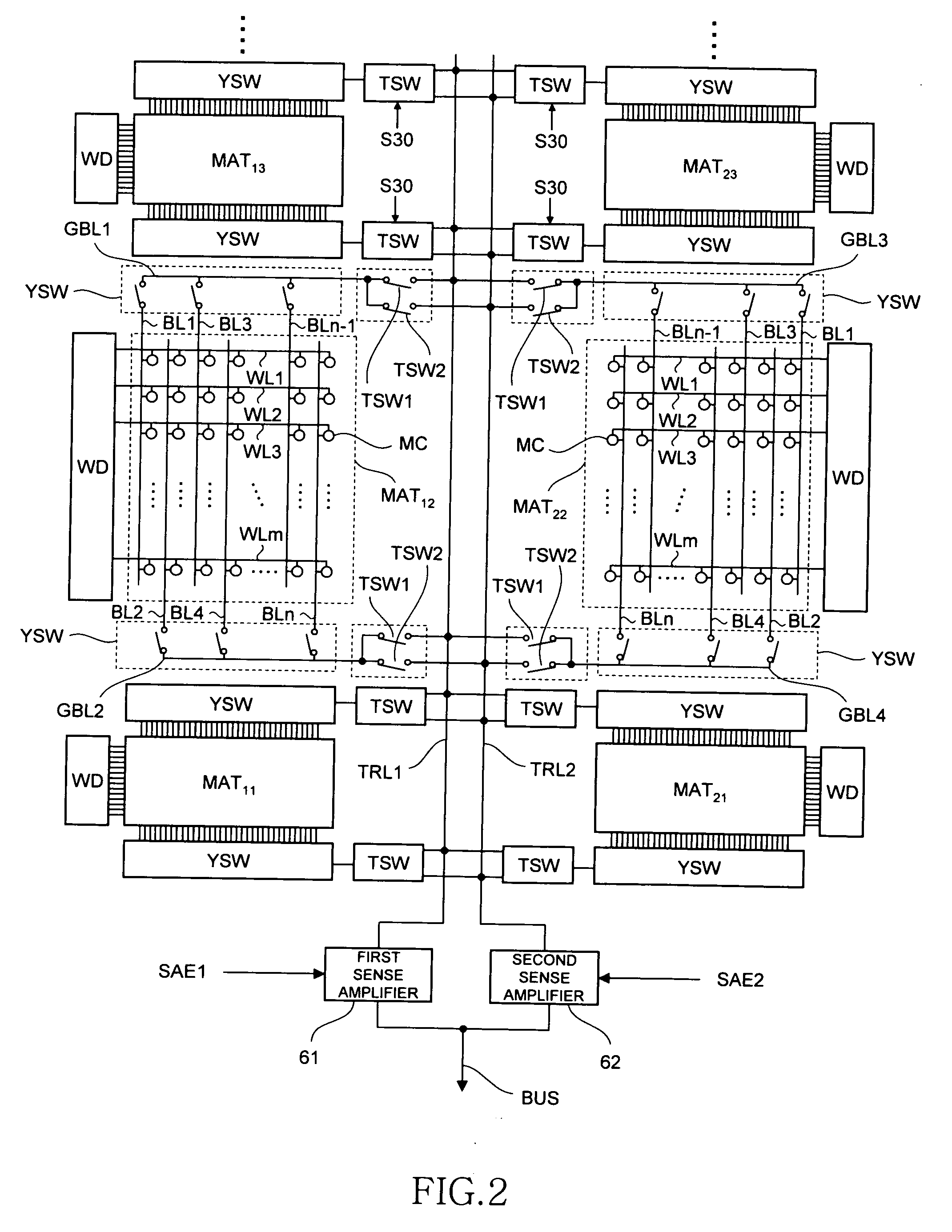
  • Figure 2
    Figure 2
  • Figure 3
    Figure 3
Patent Text Reader

Abstract

A semiconductor memory device includes: a plurality of word lines; a plurality of bit lines; plurality of memory cells arranged at intersections of the word lines and the bit lines; a word driver that selects any one of the word lines; a plurality of sense amplifiers connectable to any of the bit lines; a sense-amplifier starting circuit that sequentially starts the sense amplifiers in response to a request of consecutive read operations to the memory cells connected to a predetermined word line, in a state that the predetermined word line is selected by the word driver; and an address determining circuit that temporarily stops an operation of the sense-amplifier starting circuit in response to a request of consecutive read operations to a same memory cell connected to a predetermined word line, in a state that the predetermined word line is selected by the word driver.
Need to check novelty before this filing date? Find Prior Art

Description

BACKGROUND OF THE INVENTION

[0001] 1. Field of the Invention

[0002] The present invention relates to a semiconductor memory device and a control method thereof, and particularly relates to a semiconductor memory device including a plurality of sense amplifiers that can be connected to any of a plurality of bit lines and a control method thereof.

[0003] 2. Description of Related Art

[0004] Currently, there are various types of semiconductor memory devices, and DRAM (Dynamic Random Access Memory) can be mentioned as a representative thereof. Most of DRAMs are of a synchronous type in which data is inputted and outputted in synchronization with a clock signal, and can be randomly accessed with a cycle of about 7 ns.

[0005] However, DRAM is a volatile memory, and therefore there are problems as follows. Stored data is lost once the power supply is disconnected, and thus DRAM is not suitable for storing a program or archival data that should be saved for a long period of time. Further, even when t...

Examples

Embodiment Construction

[0031]Preferred embodiments of the present invention will be explained below in detail with reference to the accompanying drawings.

[0032]FIG. 1 is a block diagram showing a configuration of a semiconductor memory device according to a preferred embodiment of the present invention.

[0033]As shown in FIG. 1, a semiconductor memory device 10 according to the present embodiment includes a memory cell array 11 including a plurality of memory cells MC, a plurality of address terminals 21 that receive an address signal ADD, a plurality of command terminals 22 that receive a command signal CMD, a clock terminal 23 that receives an external clock signal CK, and a data terminal 24 that inputs and outputs data DQ. Although not particularly limited, the semiconductor memory device 10 is of a synchronous type which operates in synchronization with the external clock signal CK.

[0034]The address signal ADD inputted via the address terminals 21 is supplied to an address buffer 31. Among the address ...