Device and method for the inspection of defects on the edge region of a wafer

a technology for inspection and defects, applied in measurement devices, material analysis through optical means, instruments, etc., can solve the problems of unable to approach single positions and not being able to capture single images of selected defects, etc., to achieve reliable inspection of defects on the edge of the wafer

Inactive Publication Date: 2009-11-12
VISTEC SEMICON SYST
View PDF7 Cites 6 Cited by
  • Summary
  • Abstract
  • Description
  • Claims
  • Application Information

AI Technical Summary

Benefits of technology

[0008]The object of the present invention is to create a device with which a reliable inspection of defects on the edge of the wafer is possible. Thereby, the device should have the ability to examine the defects on the top surface of the edge of the wafer, on the angle of the wafer and on the bottom surface of the edge of the wafer.

Problems solved by technology

The apparatus suggested in this Korean patent application, however, is not suitable for capturing single images of selected defects.
Likewise, this device also cannot approach single positions of defects on the edge of the wafer and cannot capture images of these defects.

Method used


Image

  • Device and method for the inspection of defects on the edge region of a wafer
  • Device and method for the inspection of defects on the edge region of a wafer
  • Device and method for the inspection of defects on the edge region of a wafer

Examples


Embodiment Construction

[0047]Same reference numbers refer to same elements throughout the various figures. This should not be regarded as a limitation of the invention.

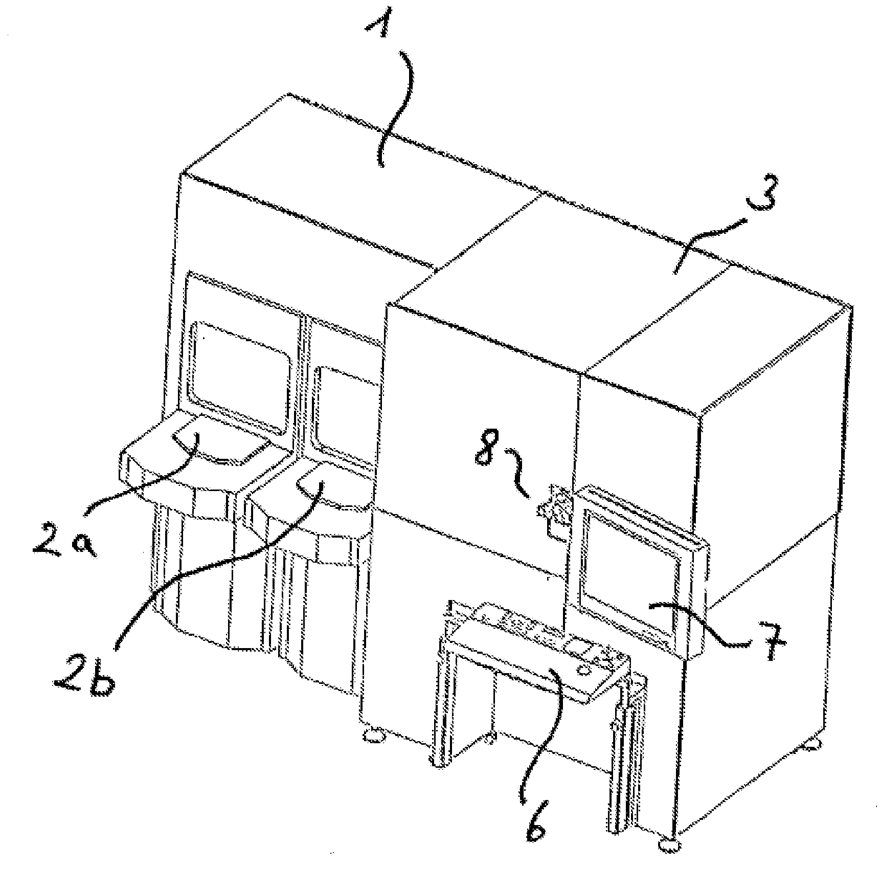
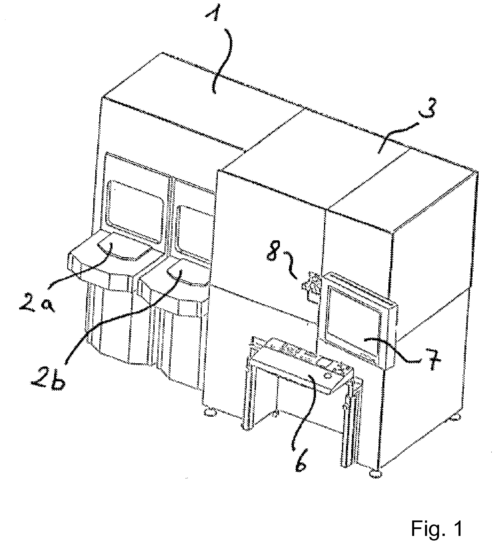
[0048]FIG. 1 shows a perspective view of an inspection device 3 for wafers, wherein the device according to the invention is used. The inspection device 3 comprises a substrate feeding module 1 and at least one working station (here not shown; see FIG. 2). Further, the inspection device 3 is provided with a monitor 7, with which the user can control his carried out inputs via the control panel 6. Likewise, the captured images of the defects on the edge of the wafer or on the top surface of the wafer itself captured by the working station or the working stations are visually displayed to the user on the monitor 7. Further, the substrate can be directly observed and examined with a microscope via a microscope ocular 8. The substrate feeding module 1 is provided on the face with a plurality of load ports 2a, 2b, via which the inspection device...


PUM

PropertyMeasurementUnit
depth of focusaaaaaaaaaa
sizeaaaaaaaaaa
sizeaaaaaaaaaa

Abstract

A method, a device and the application for the inspection of defects on the edge region of a wafer (6) is disclosed. At least one illumination device (41) illuminates the edge region (6a) of the wafer (6). At least one optical unit (40) is provided, said optical unit (40) being positionable subject to the position of the defect (88) relative to a top surface (30) of the edge of the wafer (6a) or a bottom surface (31) of the edge of the wafer (6a) or a face (32) of the edge of the wafer (6a) for capturing an image of said defect.

Description

RELATED APPLICATIONS[0001]This application is a Continuation of International Application No. PCT / EP2008 / 015339, filed on Feb. 4, 2008, which claims priority to German Patent Application Nos. DE 10 2007 013 655.4, filed on Mar. 19, 2007, and DE 10 2007 047 935.4, filed on Dec. 21, 2007, and claims the benefit under 35 USC 119(e) of U.S. Provisional Application No. 60 / 895,700, filed on Mar. 19, 2007, all of which are incorporated herein by reference in their entirety.FIELD OF THE INVENTION[0002]The present invention relates to a device for the inspection of defects on the edge region of a wafer.[0003]In addition, the invention relates to a method for the inspection of defects on the edge region of a wafer.BACKGROUND OF THE INVENTION[0004]Japanese patent application JP 2006 / 294969 A discloses an inspection equipment for wafers which captures images of the circumferential edge of the wafer. Preferably the edge region of the wafer is being inspected to that effect whether any abnormalit...

Claims


Application Information

Patent Timeline
Patent Type & Authority Applications(United States)
IPC IPC(8): G01N21/88
CPCG01N2021/8825G01N21/9503
Inventor DANNER, LAMBERTHEIDEN, MICHAELVOLLRATH, WOLFGANGBUTTNER, ALEXANDERKRAMPE-ZADLER, CHRISTOF
Owner VISTEC SEMICON SYST
Why Eureka
Try Eureka