Method of manufacturing flat panel display device

a technology of display device and flat panel, which is applied in the manufacture of electrode systems, identification means, instruments, etc., can solve the problems of reducing the sealing effect, and reducing the humidity resistance of organic sealants

Active Publication Date: 2010-02-11
SAMSUNG DISPLAY CO LTD
View PDF8 Cites 19 Cited by
  • Summary
  • Abstract
  • Description
  • Claims
  • Application Information

AI Technical Summary

Benefits of technology

[0016]Aspects of the present invention provide a method of manufacturing a flat panel display device, in which stress variations applied to mother glasses when a glass sealing material is melted to combine the mother glasses are minimized.

Problems solved by technology

Organic sealants for combining the sealing member and the substrate are susceptible to pressure.
In addition, the humidity-resistance characteristics of organic sealants quickly decrease over time, and the sealing effect is decreases.
In this method, the cut surfaces of the mother glasses may have defects due to thermal stress generated during laser beam irradiation.
As a result, various thermal impacts are applied to the mother glasses, and thus, non-uniform stresses occur in the mother glasses.
Due to non-uniform stresses, it may be difficult to cut the mother glasses accurately, and cut sides thereof may have protrusions.

Method used


Image

  • Method of manufacturing flat panel display device
  • Method of manufacturing flat panel display device
  • Method of manufacturing flat panel display device

Examples


Embodiment Construction

[0045]Reference will now be made in detail to the present embodiments of the present invention, examples of which are illustrated in the accompanying drawings, wherein like reference numerals refer to the like elements throughout. The embodiments are described below in order to explain the present invention by referring to the figures.

[0046]It is to be understood that where is stated herein that one layer is “formed on” or “disposed on” a second layer, the first layer may be formed or disposed directly on the second layer or there may be intervening layers between the first layer and the second layer. Further, as used herein, the term “formed on” is used with the same meaning as “located on” or “disposed on” and is not meant to be limiting regarding any particular fabrication process.

[0047]Hereinafter, an embodiment of the present invention will be described in detail with reference to the accompanying drawings.

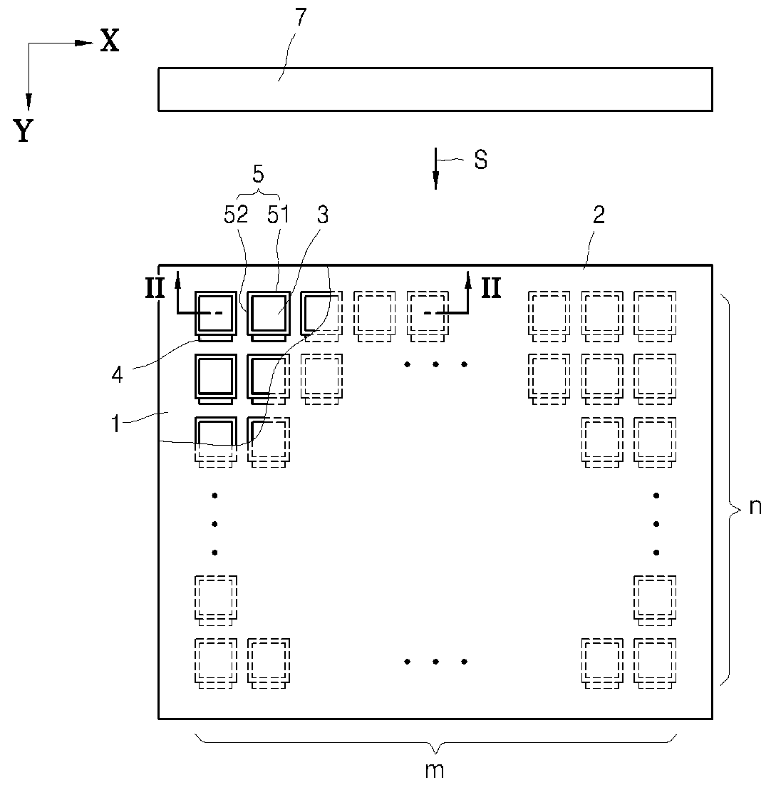
[0048]FIG. 1 a plan view of a substrate and a laser illuminator that are...


PUM

PropertyMeasurementUnit
angleaaaaaaaaaa
wavelengthaaaaaaaaaa
widthaaaaaaaaaa

Abstract

To minimize stress variations applied to mother glasses when a glass sealing material is melted via a laser to combine the mother glasses, a method of manufacturing a flat panel display device includes providing a plurality of emission units between a first substrate and a second substrate, wherein the first substrates faces the second substrate and each emission unit forms a unit display device; providing a plurality of walls between the first substrate and the second substrate, wherein each wall respectively surrounds one of the emission units; irradiating a laser beam onto the walls, wherein the laser beam is simultaneously irradiated to wall portions aligned in a row in a first direction; scanning the laser beam in a second direction, wherein the second direction is different from the first direction to irradiate other wall portions of the plurality of walls; and cutting the first and second substrates to obtain individual display devices.

Description

CROSS-REFERENCE TO RELATED APPLICATIONS[0001]This application claims the benefit of Korean Patent Application No. 2008-77552, filed on Aug. 7, 2008, in the Korean Intellectual Property Office, the disclosure of which is incorporated herein by reference.BACKGROUND OF THE INVENTION[0002]1. Field of the Invention[0003]Aspects of the present invention relate to a method of manufacturing a flat panel display device, and more particularly, to a method of manufacturing a flat panel display device sealed with a glass sealing material.[0004]2. Description of the Related Art[0005]In general, flat panel display devices such as organic light emitting display devices or thin film transistor-liquid crystal displays (TFT-LCDs) can be manufactured to have a thin and flexible structure. Because of these useful properties, research into flat panel display devices is being actively performed.[0006]Typically, organic light emitting display devices may be degraded by humidity. Accordingly, there is a ne...

Claims


Application Information

Patent Timeline
Patent Type & Authority Applications(United States)
IPC IPC(8): H01J9/26C03B33/07C03B33/09G09F9/00
CPCC03C8/24C03C27/06H01L2251/566H01L51/5237H01L51/56C03C2218/34H10K50/8426H10K71/851H10K71/00G02F1/13G02F1/1339
Inventor KIM, HYUNG-SIKPARK, JIN-HANKIM, JOON-HYUNGLEE, HYUN-CHULKIM, SUNG-GONKANG, TAE-WOOKKIM, JONG-DAEHAN, GYOO-WANROH, CHEOL-LAE
Owner SAMSUNG DISPLAY CO LTD
Why Eureka
Try Eureka