Integrated circuit package system with redistribution layer
- Summary
- Abstract
- Description
- Claims
- Application Information
AI Technical Summary
Problems solved by technology
Method used
Image

Examples
first embodiment
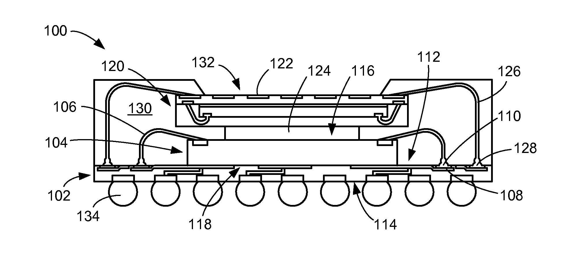
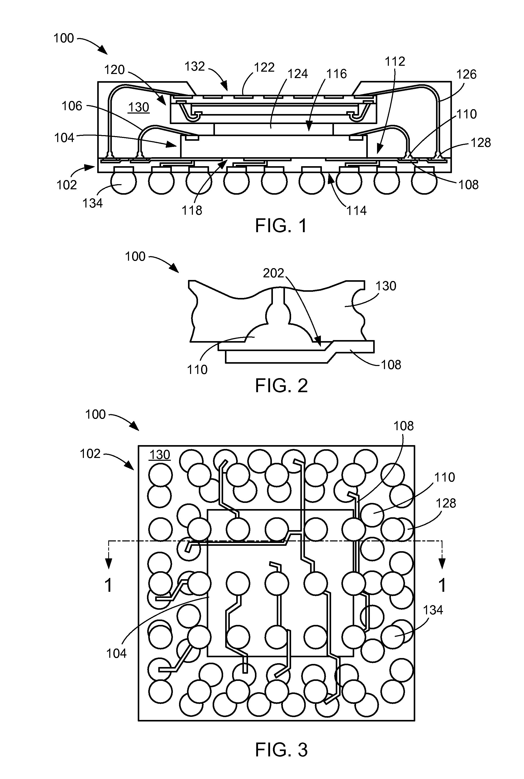
[0044]Referring now to FIG. 1, therein is shown a cross-sectional view of an integrated circuit package system 100 taken along line 1-1 of FIG. 3 in the present invention. The integrated circuit package system 100 preferably includes a redistribution network 102, a base device 104, and base interconnects 106.
[0045]The redistribution network 102 can be formed of one or more re-routing films 108 such as thin film conductors including integrated passive devices (IPD), or redistribution layers (RDL). The re-routing films 108 can be formed in a range of a few micrometers and provide an internal side 112 and an external side 114 of the redistribution network 102.
[0046]The base interconnects 106 such as wire bonds, planar interconnect, bumps, or any conductive material with any connection technology can include a base ball-end 110. The base ball-end 110 can be formed over the internal side 112 of the redistribution network 102 electrically connecting one of the re-routing films 108 to a ba...
second embodiment
[0073]Referring now to FIG. 9, therein is shown a cross-sectional view of an integrated circuit package system 900 taken along line 9-9 of FIG. 11 in the present invention. The integrated circuit package system 900 preferably includes a redistribution network 902, a base device 904, and base interconnects 906.
[0074]The redistribution network 902 can be formed of one or more re-routing films 908 such as thin film conductors including integrated passive devices (IPD), or redistribution layers (RDL). The re-routing films 908 can be formed in a range of a few micrometers and provide an internal side 912 and an external side 914 of the redistribution network 902.
[0075]The base interconnects 906 such as wire bonds, planar interconnect, bumps, or any conductive material with any connection technology can include a base ball-end 910. The base ball-end 910 can be formed over the internal side 912 of the redistribution network 902 electrically connecting one of the re-routing films 908 to a b...
third embodiment
[0100]Referring now to FIG. 17, therein is shown a cross-sectional view of an integrated circuit package system 1700 in the present invention. The integrated circuit package system 1700 preferably includes a redistribution network 1702, a base device 1704, and base interconnects 1706.
[0101]The redistribution network 1702 can be formed of one or more re-routing films 1708 such as thin film conductors including integrated passive devices (IPD), or redistribution layers (RDL). The re-routing films 1708 can be formed in a range of a few micrometers and provide an internal side 1712 and an external side 1714 of the redistribution network 1702.
[0102]The base interconnects 1706 such as wire bonds, planar interconnect, bumps, or any conductive material with any connection technology can include a base ball-end 1710. The base ball-end 1710 can be formed over the internal side 1712 of the redistribution network 1702 electrically connecting one of the re-routing films 1708 to components.
[0103]...
PUM
 Abstract
Description
Claims
Application Information
 - R&D Engineer
- R&D Manager
- IP Professional
- Industry Leading Data Capabilities
- Powerful AI technology
- Patent DNA Extraction
Browse by: Latest US Patents, China's latest patents, Technical Efficacy Thesaurus, Application Domain, Technology Topic.
© 2024 PatSnap. All rights reserved.Legal|Privacy policy|Modern Slavery Act Transparency Statement|Sitemap