

Thermal barrier layer for integrated circuit manufacture
- Summary
- Abstract
- Description
- Claims
- Application Information
AI Technical Summary
Benefits of technology
Problems solved by technology
Method used
Image

Examples
Embodiment Construction
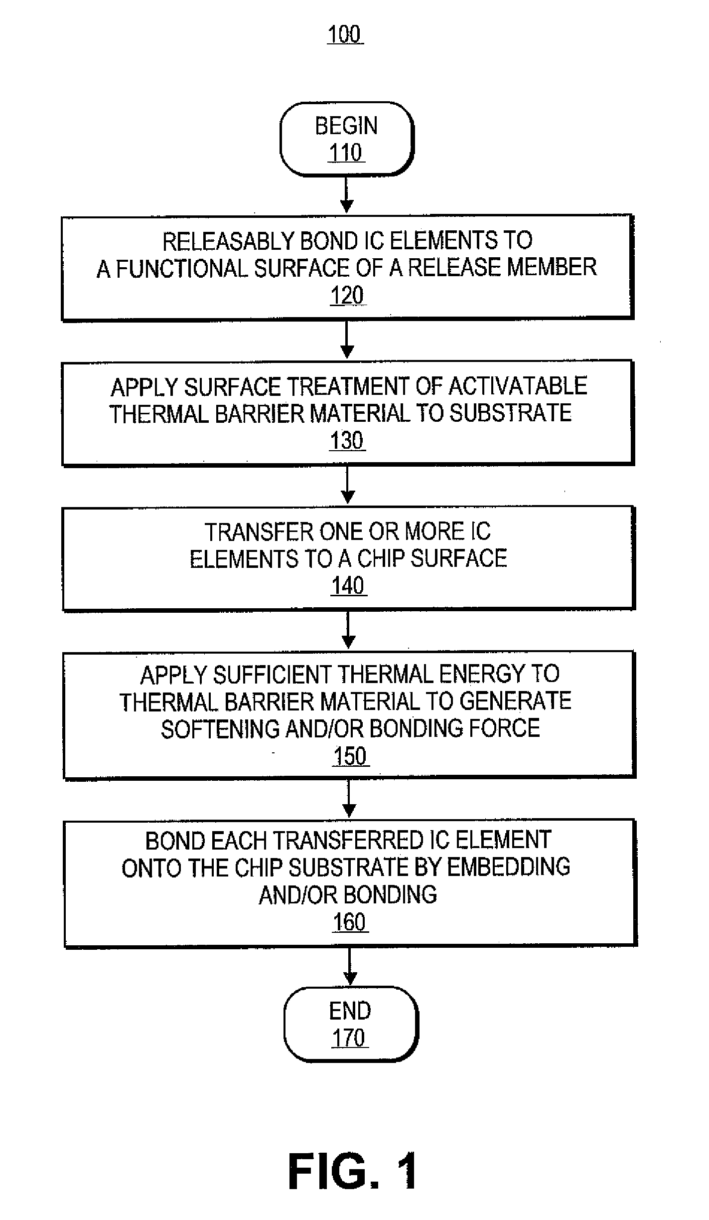
[0001]1. Field of the Invention
[0002]This invention relates generally to assembly of semiconductor devices and, more particularly, to the assembly of integrated circuit elements.
[0003]2. Background of the Invention
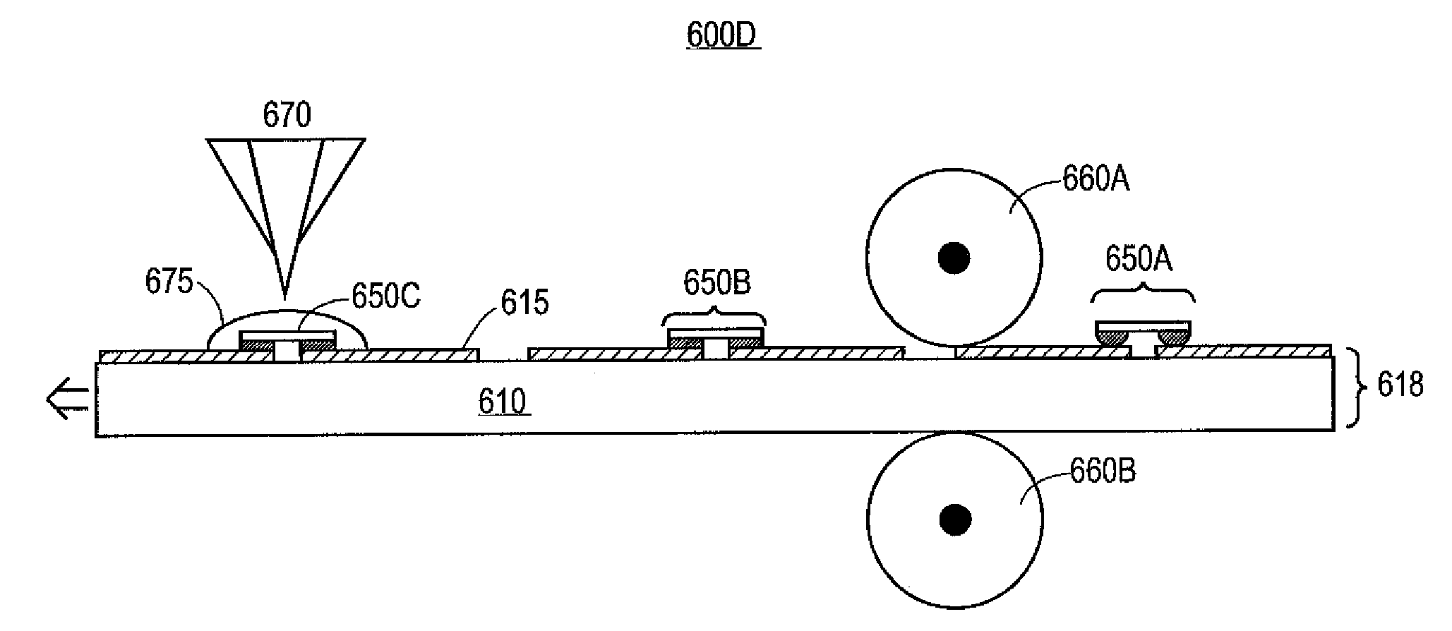
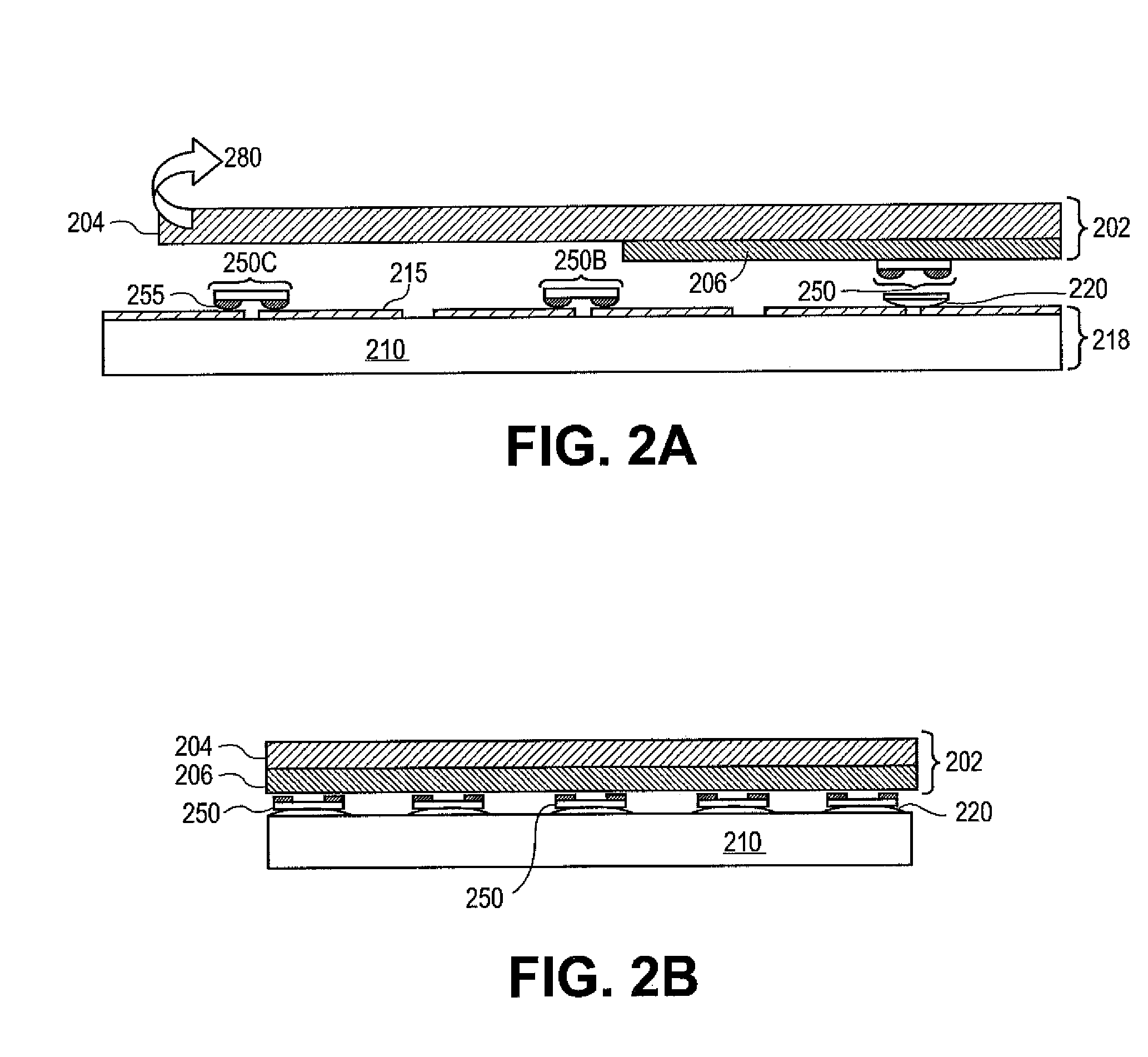
[0004]As market demand increases for integrated circuit (IC) products such as radio frequency identification (RFID) tags, and as IC die sizes shrink, high assembly throughput rates for very small die and low production costs are crucial in providing commercially-viable products. For example, the cost of an RFID device still depends on assembly complexity.
[0005]Conventional methods for assembling IC products include pick and place techniques. Such techniques involve a manipulator, such as a robot arm, to remove IC dies from a wafer and place them onto a die carrier or directly onto a substrate. The dies are ultimately mounted onto a substrate with other electronic components, such as antennas, capacitors, resistors, and inductors to form an electronic device. However, these...
PUM
| Property | Measurement | Unit |
|---|---|---|
| Pressure | aaaaa | aaaaa |
| Flexibility | aaaaa | aaaaa |
| Electrical conductor | aaaaa | aaaaa |
Abstract
Description
Claims
Application Information