
Touch screen panel integrated into liquid crystal display, method of manufacturing the same, and touch sensing method

a technology of touch screen and liquid crystal display, which is applied in the direction of instruments, computing, electric digital data processing, etc., can solve the problem of difficult recognition of multiple touches by such a touch sensor

Inactive Publication Date: 2010-04-29
SAMSUNG ELECTRONICS CO LTD
View PDF16 Cites 145 Cited by
  • Summary
  • Abstract
  • Description
  • Claims
  • Application Information

AI Technical Summary

Benefits of technology

The invention relates to an improved design for LCD displays that includes a built-in touch screen panel. This technology uses a special process called capacitive overlay to create the touch screen, resulting in better accuracy and responsiveness compared to other types of touch screens. Additionally, this patent describes methods for manufacturing and utilizing the new touch screen panels.

Problems solved by technology

The technical problem addressed in this patent relates to improving the design of touch screen panels integrated into electronic devices like computers, laptops, and PMPs. Specifically, they aim to provide better recognition of multi-touch inputs and improve the accuracy of coordinate readings without compromising the quality of the displayed image. Additionally, they also hope to reduce the impact on the aperture ratio of the display device caused by the placement of sensing lines.

Method used


Image

  • Touch screen panel integrated into liquid crystal display, method of manufacturing the same, and touch sensing method
  • Touch screen panel integrated into liquid crystal display, method of manufacturing the same, and touch sensing method
  • Touch screen panel integrated into liquid crystal display, method of manufacturing the same, and touch sensing method

Examples


Embodiment Construction

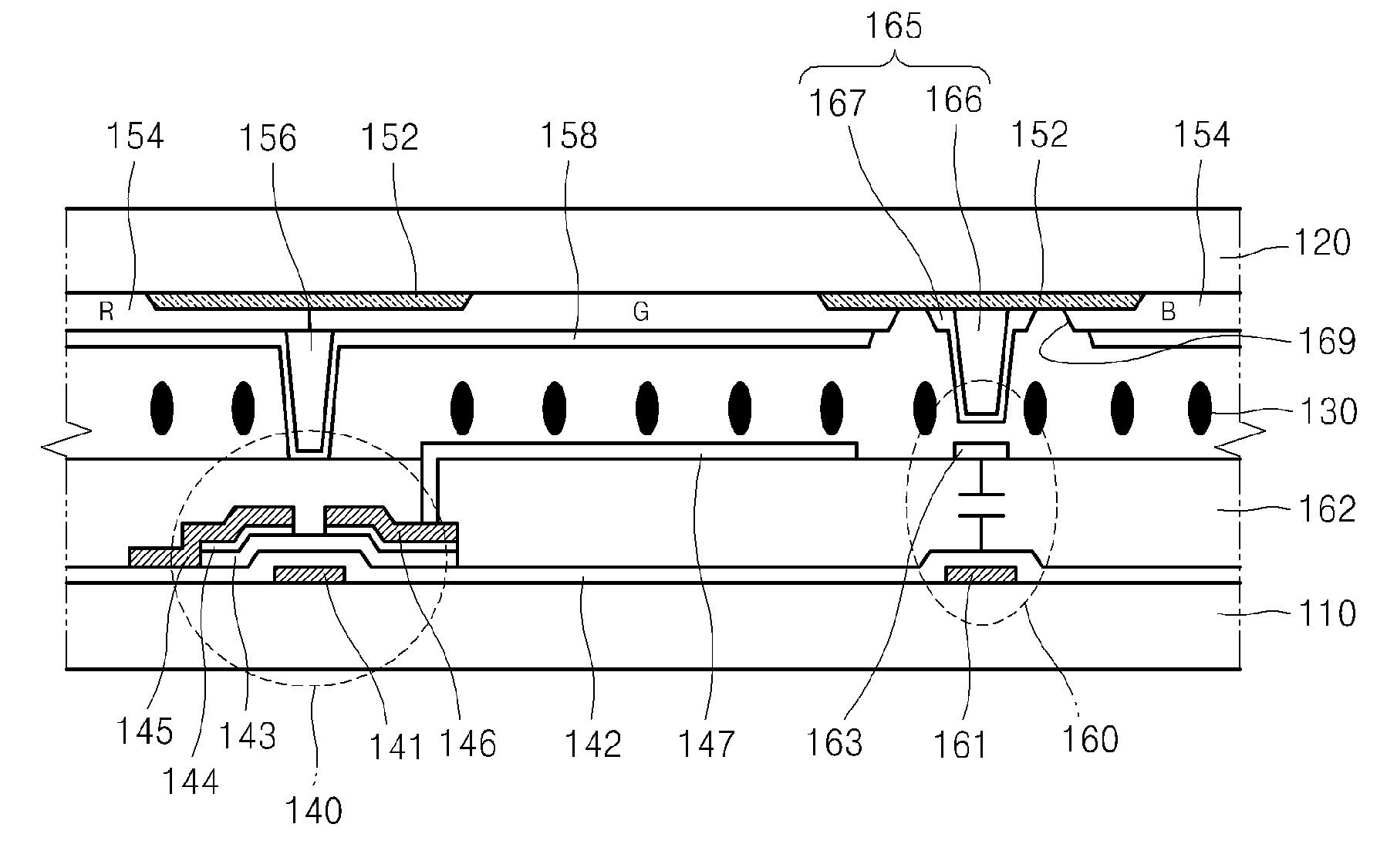
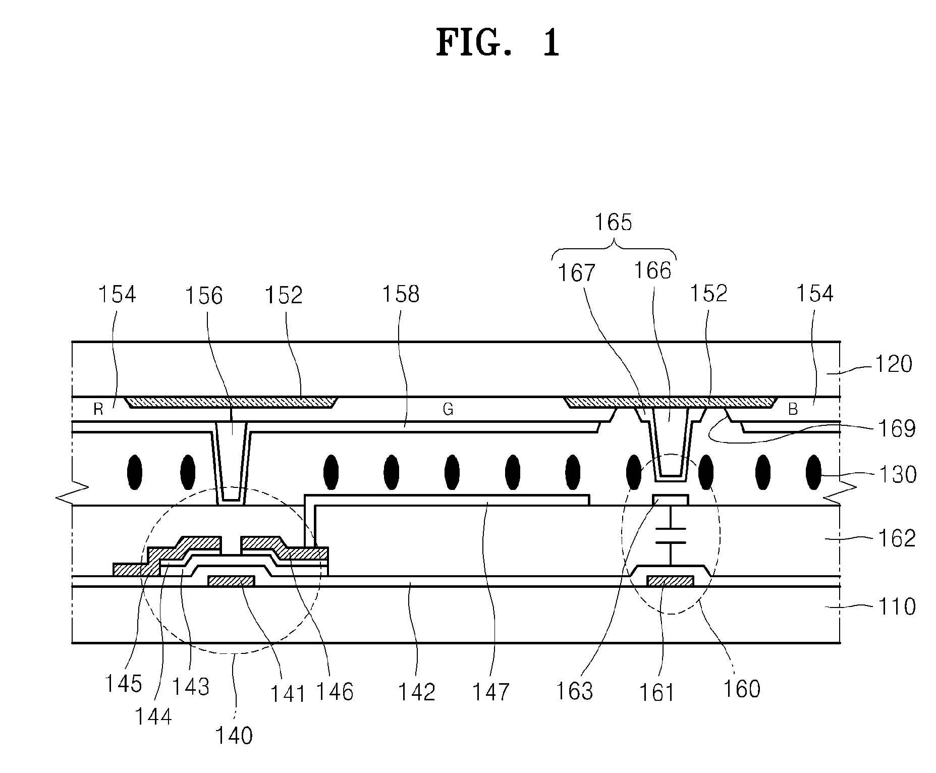
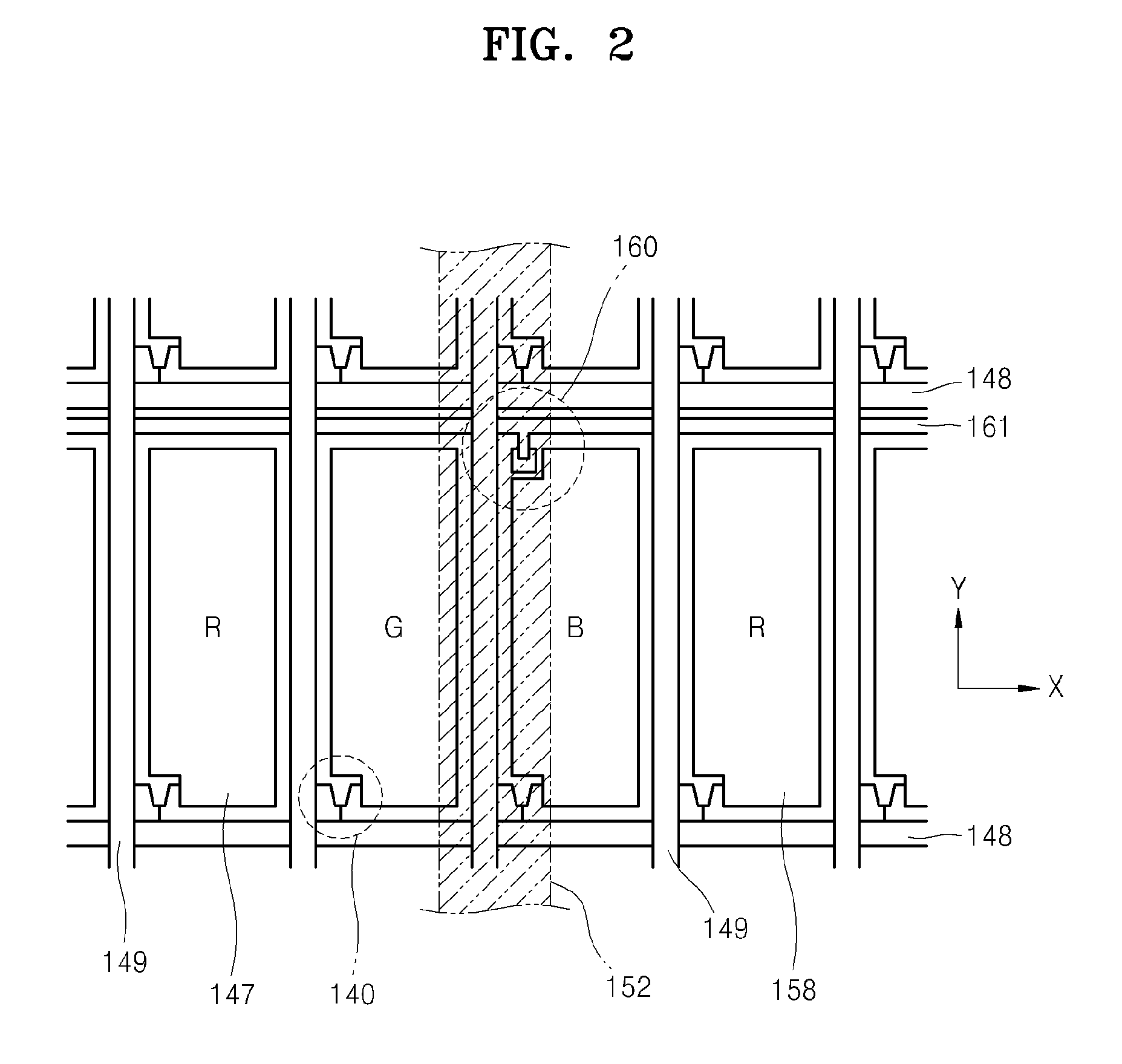
[0032]Reference is now made in detail to embodiments, examples of which are illustrated in the accompanying drawings, wherein like reference numerals refer to like elements throughout. In this regard, the present embodiments may have different forms and should not be construed as being limited to the descriptions set forth herein. Accordingly, the embodiments are merely described below, with reference to the figures, to explain aspects, advantages and features of the embodiments.

[0033]It will be understood that when an element or layer is referred to as being “on” or “connected to” another element or layer, the element or layer can be directly on or connected to another element or layer or intervening elements or layers. In contrast, when an element is referred to as being “directly on” or “directly connected to” another element or layer, there are no intervening elements or layers present. As used herein, the term “and / or” includes any and all combinations of one or more of the ass...


PUM


Abstract

A touch screen panel includes: a first substrate and a second substrate, which face each other with respect to a liquid crystal interposed therebetween; and a touch sensor interposed between the first substrate and the second substrate. The touch sensor includes: a plurality of first touch signal lines disposed on the first substrate and extending in a first direction; a protective layer disposed on the first substrate, the protective layer including a dielectric material and substantially the plurality of first touch signal lines; a plurality of contact pads disposed on the protective layer; a plurality of second touch signal lines disposed on the second substrate and extending in a second direction perpendicular to the first direction; and a plurality of touch sensor spacers electrically connected to the plurality of second touch signal lines. A gap between the touch sensor spacers and the plurality of contact pads is defined, and the spacers are disposed to face the plurality of contact pads.

Description


Claims


Application Information

Patent Timeline
Owner SAMSUNG ELECTRONICS CO LTD
Features
  • Generate Ideas
  • Intellectual Property
  • Life Sciences
  • Materials
  • Tech Scout
  • Unparalleled Data Quality
  • Higher Quality Content
  • 60% Fewer Hallucinations
Learn More