Electronic circuit with embedded memory

a technology of embedded memory and electronic circuits, applied in the field of circuitry, can solve the problems of large chip area consumed by laterally oriented devices, large amount of chip area consumed by lateral oriented devices, and large amount of processing circuits idle for many cycle times,

Inactive Publication Date: 2010-06-03
BESANG
View PDF99 Cites 217 Cited by
  • Summary
  • Abstract
  • Description
  • Claims
  • Application Information

AI Technical Summary

Problems solved by technology

However, these laterally oriented devices consume significant amounts of chip area.
As a result, the processor circuit is idle for many cycle times while it accesses the main memory.
Hence, cache memory uses a small amount of fast and expensive memory to allow the processor circuit faster access to information normally stored by a large amount of slower, less-expensive memory.
However, there are several problems with doing this.
One problem with doing this is cost.
As mentioned above, the SRAM cells included in cache memory are larger and expensive, so increasing the size of the cache memory would significantly increase the cost of the computer chip.
DRAM cells are less expensive and smaller, but to embed them with the main computer chip will still significantly increase the cost.
One reason the cost increases for both embedded SRAM and DRAM cells is because the number of masks needed to fabricate the main computer chip increases.
This is because the masks used to fabricate the processor and control circuitry are not compatible with the masks used to fabricate SRAM and DRAM memory cells.
Another reason the cost increases is because, as discussed below, the yield in manufacturing computer chips decreases as the size of the computer chip increases.
Another problem is that in today's computer systems, the size of the main memory is much larger than the size of the cache memory.
Thus, to increase the size of the cache memory by increasing the number of SRAM cells included therein would significantly increase the size of the computer chip and decrease its yield.
This presents several problems.
As mentioned above, one problem is that the yield of computer chips in a manufacturing run decreases as their size increases.
A wafer, however, has defects distributed throughout it surface which can negatively impact the operation of the computer chips.
Further, if the computer chip is smaller in size, then more of them can be fabricated from a single wafer, which also decreases costs.
Hence, smaller computer chips increase the yield and decrease the costs.
Another problem is that it is typically desirable to increase the number of devices included in the processor and control circuitry so that the processor can operate faster and perform more complicated operations.
In one way, the computer chip can include devices which are smaller, but this requires advances in lithography and increasingly expensive manufacturing equipment.
The total area of the computer chip can be increased, but as discussed above, this decreases the yield and increases the cost.

Method used


Image

  • Electronic circuit with embedded memory
  • Electronic circuit with embedded memory
  • Electronic circuit with embedded memory

Examples


Embodiment Construction

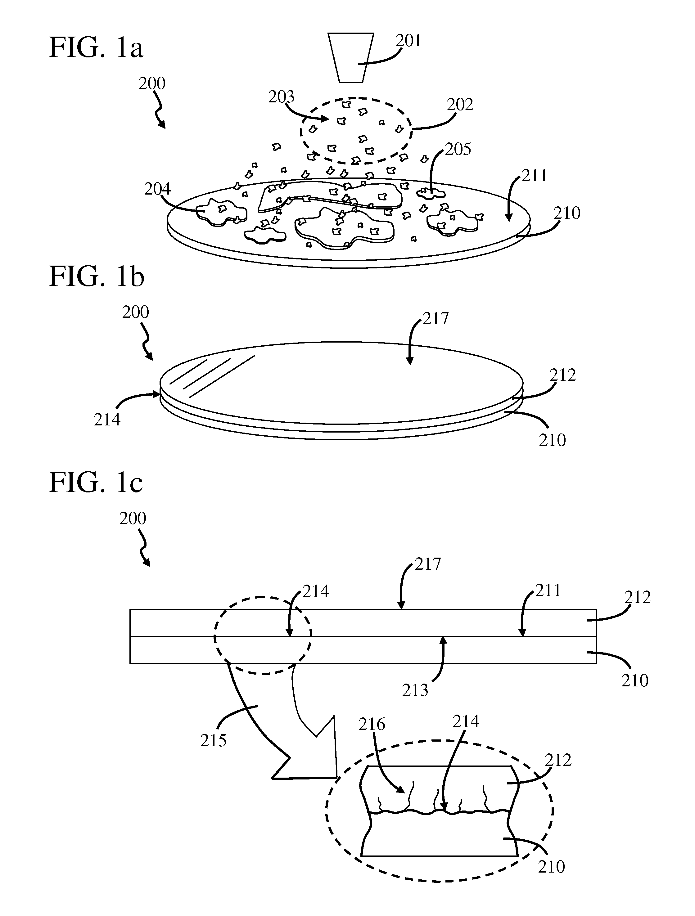
[0050]FIG. 1a is a perspective view of a partially fabricated grown semiconductor structure 200. It should be noted that in the following figures, like reference characters indicate corresponding elements throughout the several views. Grown semiconductor structure 200 includes a substrate 210. Substrate 210 can be of many different types, such as a semiconductor substrate.

[0051]In this embodiments, a gaseous semiconductor material 203 is provided from a growth material source 201 in a region 202 proximate to a substrate surface 211 of substrate 210. It should be noted that, in general, more than one material sources are used to provide growth material and process gases. However, one material source is shown in FIG. 1a for simplicity and ease of discussion.

[0052]Portions of gaseous semiconductor material 203 engage surface 211 to form agglomerated semiconductor material 204 and 205. Portions of gaseous semiconductor material 203 engage surface 211 to form a grown semiconductor layer ...


PUM


Abstract

Circuitry includes first and second circuits spaced apart by an interconnect region. The interconnect region includes a first interconnect, and the second circuit includes a stack of semiconductor layers. The first interconnect extends between the first and second circuits to provide communication therebetween. The second circuit operates as a memory circuit.

Description

CROSS-REFERENCE TO RELATED APPLICATIONS[0001]This application is a continuation-in-part of, and claims the benefit of, U.S. patent application Ser. No. 11 / 092,521, which was filed on Mar. 29, 2005 by the same inventor, the contents of which are incorporated by reference as though fully set forth herein.[0002]This application is a continuation-in-part of, and claims the benefit of, U.S. patent application Nos.:[0003]Ser. No. 12 / 165,445; and[0004]Ser. No. 12 / 165,475;which in turn are divisionals of, and claim the benefit of, U.S. patent application Ser. No. 11 / 092,499 (now U.S. Pat. No. 7,470,598), filed on Mar. 29, 2005, which is a continuation-in-part of, and claims the benefit of, claims the benefit of U.S. patent application Ser. No. 10 / 873,969 (now U.S. Pat. No. 7,052,941), filed on Jun. 21, 2004.[0005]This application is a continuation-in-part of, and claims the benefit of, U.S. patent application Nos.:[0006]Ser. No. 11 / 092,500, filed on Mar. 29, 2005,[0007]Ser. No. 11 / 092,501, ...

Claims


Application Information

Patent Timeline
Patent Type & Authority Applications(United States)
IPC IPC(8): H01L23/522
CPCH01L21/2007H01L21/8221H01L2924/1301H01L2924/1306H01L2924/01033H01L24/83H01L27/0688H01L2224/291H01L2224/8385H01L2924/01013H01L2924/01015H01L2924/01027H01L2924/01029H01L2924/01049H01L2924/01051H01L2924/01074H01L2924/01093H01L2924/07802H01L2924/13091H01L2924/14H01L2924/19041H01L2924/19042H01L2924/19043H01L2924/30105H01L24/29H01L2924/01021H01L2924/00
Inventor LEE, SANG-YUN
Owner BESANG
Why Eureka
Try Eureka