Electronic component placing apparatus and electronic component mounting method

a technology of electronic components and placing apparatuses, which is applied in the direction of soldering apparatus, sustainable manufacturing/processing, final product manufacturing, etc., can solve the problems of gap with the electrode of the board, warp deformation, and cold join

Inactive Publication Date: 2010-07-01
PANASONIC CORP
View PDF14 Cites 13 Cited by
  • Summary
  • Abstract
  • Description
  • Claims
  • Application Information

AI Technical Summary

Benefits of technology

[0009]With the invention, in the film formation operation performed before the paste transfer step of supplying the solder paste to the solder bumps, it is possible to prevent a cold joint from occurring when the electronic component likely to cause warp deformation is mounted by means of soldering by forming a film having a film thickness distribution for transferring a desired transfer amount of solder paste according to the state of warp deformation in the reflow process of the electronic component to each of the plurality of solder bumps.

Problems solved by technology

Therefore, the circuit board or the semiconductor package placed on this circuit board has lower rigidity, and is likely to cause warp deformation by heating.
Therefore, in a reflow process after placing the semiconductor package with solder bumps formed on the lower surface on the board, the solder bump in a portion where the warp deformation occurs tends to float and cause a gap with the electrode of the board.
As a result, the solder bumps are not normally joined by soldering with the connecting electrodes on the board, likely producing a cold joint such as faulty electrical continuity or insufficient joint strength.

Method used


Image

  • Electronic component placing apparatus and electronic component mounting method
  • Electronic component placing apparatus and electronic component mounting method
  • Electronic component placing apparatus and electronic component mounting method

Examples


Embodiment Construction

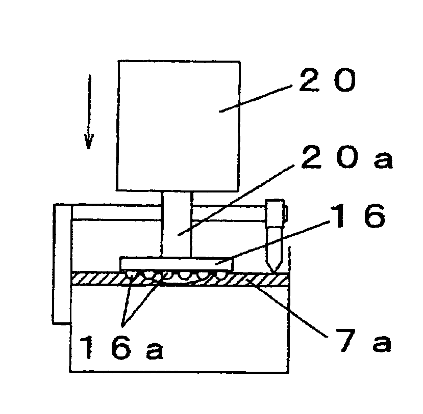
[0024]The embodiments of the present invention will be described below with reference to the drawings.

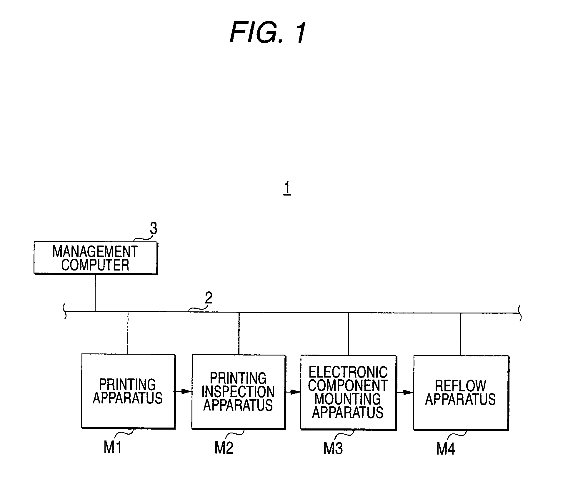
[0025]Referring to FIG. 1, first of all, an electronic component mounting system will be described below. In FIG. 1, the electronic component mounting system has an electronic component mounting line 1 connected via a communication network 2, the electronic mounting line composed of a printing apparatus M1, a printing inspection apparatus M2, an electronic component placing apparatus M3 and a reflow apparatus M4, each of which is an electronic component mounting apparatus, and is totally controlled by a management computer 3. In this embodiment, with these plurality of electronic component mounting apparatuses, an electronic component with a plurality of solder bumps for connection to the outside formed on a lower surface is mounted on a board by means of soldering to manufacture a mounted board. The electronic component mounting apparatuses may be connected via the communication ne...


PUM

PropertyMeasurementUnit
thickness distributionaaaaaaaaaa
sizeaaaaaaaaaa
mounting densityaaaaaaaaaa

Abstract

To provide an electronic component placing apparatus and an electronic component mounting method that can prevent a cold joint from occurring when an electronic component likely to cause warp deformation is mounted by means of soldering.
In the electronic component placing apparatus for placing the electronic component 16 with a plurality of solder bumps 16a formed on a lower surface on a board, a film 7a having a film thickness distribution for transferring a desired transfer amount of solder paste according to a state of warp deformation to each of the plurality of solder bumps is formed in a paste transfer unit 24, based on the component warp information indicating the state of warp deformation in a reflow process of the electronic component. Thereby, it is possible to prevent a cold joint from occurring when the electronic component likely to cause warp deformation is mounted by means of soldering by additionally supplying a just enough amount of solder to each solder bump 16a.

Description

TECHNICAL FIELD [0001]The present invention relates to an electronic component placing apparatus and an electronic component mounting method for placing an electronic component with solder bumps formed on a board and mounting it by means of soldering.BACKGROUND ART [0002]A method of mounting an electronic component such as a semiconductor device on a circuit board is used in the form of mounting a semiconductor package in which the semiconductor device is mounted on a resin board via solder bumps on the circuit board by means of soldering. In the solder joint for joining the electronic component via solder bumps to the board, the solder bumps are made to land on the electrodes of the board in a state where a solder joint auxiliary agent such as a flux or solder paste is supplied to the solder bumps. Therefore, a device for transferring the flux or solder paste is disposed in the electronic component placing apparatus (e.g., refer to patent document 1).[0003][Patent document 1] JP-A-...

Claims


Application Information

Patent Timeline
Patent Type & Authority Applications(United States)
IPC IPC(8): B23K31/02B23K3/08
CPCB23K3/0623B23K2201/40H05K3/3436H05K3/3484H05K2201/035H05K2201/094H05K2203/0139H05K2203/0338Y02P70/613H01L2224/81B23K2101/40H05K3/3485Y02P70/50
Inventor OKAMOTO, KAZUONISHI, SYOICHIMORITA, TAKESHIHIYOSHI, MASANORITOMOYASU, KAZUHIKO
Owner PANASONIC CORP
Why Eureka
Try Eureka